Condividi:        

schede memoria compatibili per hp

Se il modem non funziona, hai problemi con la scheda video o non sai che processore scegliere entra qui!!

Moderatori: m.paolo, Caffey

schede memoria compatibili per hp

Postdi LUCKYGYVER » 09/09/09 17:32

Ciao ragazzi sono nuovo e mi piace molto questo forum così mi sono iscritto.
il mio problema è questo: ho un pc HP PAVILLON t630.it con soli 512 MB di RAM ampliabili fino a 2 GB. Volevo ampliarli ma non so se devo prendere quelle HP cioè DDR SDRAM oppure posso prendere quelle compatibili che costano pure meno. Di compatibili ve ne sono tanti tipi e non tutte dovrebbero andare bene. Vorrei sapere se qualcuno ha avuto il mio stesso problema. Grazie a chi mi vorrà rispondere.
LUCKYGYVER
Newbie
 
Post: 6
Iscritto il: 09/09/09 15:05

Sponsor
 

Re: schede memoria compatibili per hp

Postdi quizface » 09/09/09 17:58

Dovresti prendere un modulo con le stesse caratteristiche di quello che hai
Scarica cpu-z vedi cosa ti dice
Se non siete sicuri di quello che scrivete, non scrivete niente, nessuno vi obbliga ed eviterete di confondere chi gia' e' confuso. Ciao..ciao
Avatar utente
quizface
Utente Senior
 
Post: 15071
Iscritto il: 03/10/04 00:36

Re: schede memoria compatibili per hp

Postdi LUCKYGYVER » 09/09/09 18:06

ho provato ma non me lo scarica perchè non trovato sul server
LUCKYGYVER
Newbie
 
Post: 6
Iscritto il: 09/09/09 15:05

Re: schede memoria compatibili per hp

Postdi quizface » 09/09/09 18:25

Se non siete sicuri di quello che scrivete, non scrivete niente, nessuno vi obbliga ed eviterete di confondere chi gia' e' confuso. Ciao..ciao
Avatar utente
quizface
Utente Senior
 
Post: 15071
Iscritto il: 03/10/04 00:36

Re: schede memoria compatibili per hp

Postdi LUCKYGYVER » 09/09/09 19:23

SCARICATO!!!! OLTRE AI mhz che sono 200 quali sono i dati salienti per verificare il tipo di scheda da cercare?
LUCKYGYVER
Newbie
 
Post: 6
Iscritto il: 09/09/09 15:05

Re: schede memoria compatibili per hp

Postdi quizface » 09/09/09 22:46

in pratica nel menu' SPD ti dice tutto

Immagine

nel caso in figura, nel primo slot DDR PC3200 (di marca G.Skill) unregistred unbuffed
Se non siete sicuri di quello che scrivete, non scrivete niente, nessuno vi obbliga ed eviterete di confondere chi gia' e' confuso. Ciao..ciao
Avatar utente
quizface
Utente Senior
 
Post: 15071
Iscritto il: 03/10/04 00:36

Re: schede memoria compatibili per hp

Postdi LUCKYGYVER » 10/09/09 09:13

grazie sei molto gentile!!!! ho visto e ci sono 2 slot dove solo la prima è occupata da SAMSUNG DDR PC 3200 (200 Mhz) da 512 Mb. Costano molto rispetto alle altre. Ma per l'HP le schede devono avere uguale capacità o possono esssere diverse. Secondo problema quali sono le schede compatibili con le Samsung coì ne metto una da 2 Gb che è la max memoria consentita. Grazie ancora
LUCKYGYVER
Newbie
 
Post: 6
Iscritto il: 09/09/09 15:05

Re: schede memoria compatibili per hp

Postdi quizface » 10/09/09 10:36

Che scheda madre hai? lo vedi nel mainboard menu' di CPU-Z

non credo che supporti schedine DDR da 2 Giga, ma al massimo da 1 Giga (e non sono sicuro nemmeno di questo)
Posta la scheda madre che vediamo
Se non siete sicuri di quello che scrivete, non scrivete niente, nessuno vi obbliga ed eviterete di confondere chi gia' e' confuso. Ciao..ciao
Avatar utente
quizface
Utente Senior
 
Post: 15071
Iscritto il: 03/10/04 00:36

Re: schede memoria compatibili per hp

Postdi LUCKYGYVER » 10/09/09 10:57

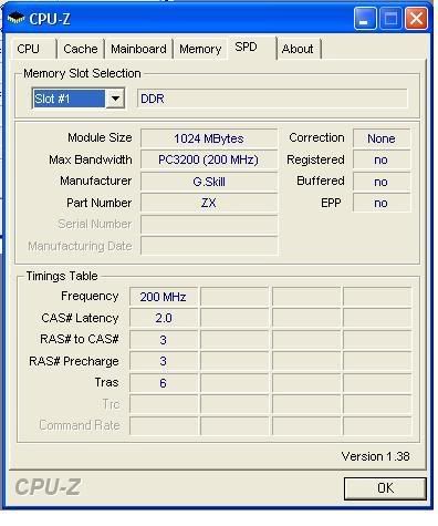
Questo è il report salvato.

CPU-Z

Binaries
CPU-Z version 1.52.2

Processors
Number of processors 1
Number of threads 1

APICs
Processor 0
-- Core 0
-- Thread 0 0

Processors Information
Processor 1 ID = 0
Number of cores 1 (max 1)
Number of threads 1 (max 1)
Name AMD Athlon 64 3200+
Codename ClawHammer
Specification AMD Athlon(tm) 64 Processor 3200+
Package Socket 754
CPUID F.4.A
Extended CPUID F.4
Brand ID 4
Core Stepping SH7-CG
Technology 0.13 um
Core Speed 1995.1 MHz
Multiplier x FSB 10.0 x 199.5 MHz
HT Link speed 598.5 MHz
Stock frequency 2000 MHz
Instructions sets MMX (+), 3DNow! (+), SSE, SSE2, x86-64
L1 Data cache 64 KBytes, 2-way set associative, 64-byte line size
L1 Instruction cache 64 KBytes, 2-way set associative, 64-byte line size
L2 cache 1024 KBytes, 16-way set associative, 64-byte line size
FID/VID Control yes
Max FID 10.0x

K8 Thermal sensor yes
K8 Revision ID 2.5
Attached device PCI device at bus 0, device 24, function 0
Attached device PCI device at bus 0, device 24, function 1
Attached device PCI device at bus 0, device 24, function 2
Attached device PCI device at bus 0, device 24, function 3


Thread dumps
CPU Thread 0
APIC ID 0
Topology Processor ID 0, Core ID 0, Thread ID 0
Type 02002001h
Max CPUID level 00000001h
Max CPUID ext. level 80000018h
Cache descriptor Level 1, I, 64 KB, 1 thread(s)
Cache descriptor Level 1, D, 64 KB, 1 thread(s)
Cache descriptor Level 2, U, 1 MB, 1 thread(s)

CPUID
0x00000000 0x00000001 0x68747541 0x444D4163 0x69746E65
0x00000001 0x00000F4A 0x00000800 0x00000000 0x078BFBFF
0x80000000 0x80000018 0x68747541 0x444D4163 0x69746E65
0x80000001 0x00000F4A 0x0000010A 0x00000000 0xE1D3FBFF
0x80000002 0x20444D41 0x6C687441 0x74286E6F 0x3620296D
0x80000003 0x72502034 0x7365636F 0x20726F73 0x30303233
0x80000004 0x0000002B 0x00000000 0x00000000 0x00000000
0x80000005 0xFF08FF08 0xFF20FF20 0x40020140 0x40020140
0x80000006 0x00000000 0x42004200 0x04008140 0x00000000
0x80000007 0x00000000 0x00000000 0x00000000 0x0000000F
0x80000008 0x00003028 0x00000000 0x00000000 0x00000000
0x80000009 0x00000000 0x00000000 0x00000000 0x00000000
0x8000000A 0x00000000 0x00000000 0x00000000 0x00000000
0x8000000B 0x00000000 0x00000000 0x00000000 0x00000000
0x8000000C 0x00000000 0x00000000 0x00000000 0x00000000
0x8000000D 0x00000000 0x00000000 0x00000000 0x00000000
0x8000000E 0x00000000 0x00000000 0x00000000 0x00000000
0x8000000F 0x00000000 0x00000000 0x00000000 0x00000000
0x80000010 0x00000000 0x00000000 0x00000000 0x00000000
0x80000011 0x00000000 0x00000000 0x00000000 0x00000000
0x80000012 0x00000000 0x00000000 0x00000000 0x00000000
0x80000013 0x00000000 0x00000000 0x00000000 0x00000000
0x80000014 0x00000000 0x00000000 0x00000000 0x00000000
0x80000015 0x00000000 0x00000000 0x00000000 0x00000000
0x80000016 0x00000000 0x00000000 0x00000000 0x00000000
0x80000017 0x00000000 0x00000000 0x00000000 0x00000000
0x80000018 0x00000000 0x00000000 0x00000000 0x00000000

MSR 0x0000001B 0x00000000 0xFEE00900
MSR 0xC001001E 0x00000000 0x00000025
MSR 0xC0010015 0x00000000 0x0C000000
MSR 0xC0010042 0x00000200 0x000C0C0C
MSR 0xC0010041 0x000000C8 0x0000000C


Chipset
Northbridge NVIDIA nForce3 150 rev. A4
Southbridge NVIDIA nForce3 MCP rev. F6
Graphic Interface AGP
AGP Revision 3.0
AGP Transfer Rate 8x
AGP SBA supported, enabled
Memory Type DDR
Memory Size 512 MBytes
Channels Single
Memory Frequency 199.5 MHz (CPU/10)
CAS# latency (CL) 3.0
RAS# to CAS# delay (tRCD) 3
RAS# Precharge (tRP) 3
Cycle Time (tRAS) 8
Bank Cycle Time (tRC) 11
DRAM Idle Timer 16
Command Rate (CR) 2T

Memory SPD
DIMM # 1
SMBus address 0x50
Memory type DDR
Manufacturer (ID) Samsung (CE00000000000000)
Size 512 MBytes
Max bandwidth PC3200 (200 MHz)
Part number M3 68L6423ETM-CCC
Serial number F201DF54
Manufacturing date Week 39/Year 04
Number of banks 2
Data width 64 bits
Correction None
Registered no
Buffered no
Nominal Voltage 2.50 Volts
EPP no
XMP no
JEDEC timings table CL-tRCD-tRP-tRAS-tRC @ frequency
JEDEC #1 2.5-3-3-7-0 @ 166 MHz
JEDEC #2 3.0-3-3-8-0 @ 200 MHz
SPD registers
00 01 02 03 04 05 06 07 08 09 0A 0B 0C 0D 0E 0F
00 80 08 07 0D 0A 02 40 00 04 50 65 00 82 08 00 01
10 0E 04 18 01 02 20 C0 60 70 00 00 3C 28 3C 28 40
20 60 60 40 40 00 00 00 00 00 37 46 28 28 50 00 00
30 00 00 00 00 00 00 00 00 00 00 00 00 00 00 10 7E
40 CE 00 00 00 00 00 00 00 02 4D 33 20 36 38 4C 36
50 34 32 33 45 54 4D 2D 43 43 43 20 4D 45 04 27 F2
60 01 DF 54 00 53 42 43 30 33 30 30 00 00 00 00 00
70 00 00 00 00 00 00 00 00 00 00 00 00 00 00 00 00
80 00 24 B6 72 67 39 FF FF FF FF FF 09 09 49 FF FF
90 FF FF FF FF FF FF FF FF FF FF FF FF FF FF FF FF
A0 FF FF FF FF FF FF FF FF FF FF FF FF FF FF FF FF
B0 FF FF FF FF FF FF FF FF FF FF FF FF FF FF FF FF
C0 FF FF FF FF FF FF FF FF FF FF FF FF FF FF FF FF
D0 FF FF FF FF FF FF FF FF FF FF FF FF FF FF FF FF
E0 FF FF FF FF FF FF FF FF FF FF FF FF FF FF FF FF
F0 FF FF FF FF FF FF FF FF FF FF FF FF FF FF FF FF


Monitoring
Mainboard Model Diablo (0x0000024B - 0x0075C5E0)

LPCIO
LPCIO Vendor ITE
LPCIO Model IT8712
LPCIO Vendor ID 0x90
LPCIO Chip ID 0x8712
LPCIO Revision ID 0x6
Config Mode I/O address 0x2E
Config Mode LDN 0x4
Config Mode registers
00 01 02 03 04 05 06 07 08 09 0A 0B 0C 0D 0E 0F
00 00 00 00 00 00 00 00 04 00 00 00 00 00 00 00 00
10 00 00 00 00 00 00 00 00 00 00 00 00 00 00 00 00
20 87 12 06 01 00 00 40 00 01 00 01 00 00 00 00 00
30 01 00 00 00 00 00 00 00 00 00 00 00 00 00 00 00
40 00 00 00 00 00 00 00 00 00 00 00 00 00 00 00 00
50 00 00 00 00 00 00 00 00 00 00 00 00 00 00 00 00
60 0D 00 0C 00 00 00 00 00 00 00 00 00 00 00 00 00
70 09 02 00 00 04 04 00 00 00 00 00 00 00 00 00 00
Register space LPC, base address = 0x0D00


Hardware Monitors
Hardware monitor ITE IT87
Temperature 1 47°C (116°F) [0x2F] (TMPIN1)
Fan 0 874 RPM [0xC1] (FANIN0)
Register space LPC, base address = 0x0D00

00 01 02 03 04 05 06 07 08 09 0A 0B 0C 0D 0E 0F
00 13 00 FF 00 37 FF 05 37 FF 07 00 0B 00 C1 FF FF
10 FF FF FF 33 87 3A 3A 00 00 FF FF FF FF FF FF FF
20 FF FF FF FF FF FF FF FF FF 80 2F 80 FF FF FF FF
30 FF FF FF FF FF FF FF FF FF FF FF FF FF FF FF FF
40 7F 00 41 37 7F 00 FF FF 2D FF FF FF FF FF FF FF
50 00 10 7F 7F 7F FF 56 56 90 56 FE 12 00 00 00 00
60 7F 7F 7F 00 00 FF FF FF 7F 7F 7F 00 00 FF FF FF
70 7F 7F 7F 00 00 FF FF FF FF FF FF FF FF FF FF FF
80 13 00 00 00 37 FF 05 37 FF 07 00 0B 00 C1 FF FF
90 FF FF FF 33 87 3A 3A 00 00 FF FF FF FF FF FF FF
A0 FF FF FF FF FF FF FF FF FF 80 2F 80 FF FF FF FF
B0 FF FF FF FF FF FF FF FF FF FF FF FF FF FF FF FF
C0 7F 00 41 37 7F 00 FF FF 2D FF FF FF FF FF FF FF
D0 00 10 7F 7F 7F FF 56 56 90 56 FE 12 00 00 00 00
E0 7F 7F 7F 00 00 FF FF FF 7F 7F 7F 00 00 FF FF FF
F0 7F 7F 7F 00 00 FF FF FF FF FF FF FF FF FF FF FF

Hardware monitor AMD Athlon 64 3200+
Temperature 0 54°C (129°F) [0x67] (Core #0)


PCI Device
Description Host Bridge
Location bus 0 (0x00), device 0 (0x00), function 0 (0x00)
Common header
Vendor ID 0x10DE
Model ID 0x00D1
Revision ID 0xA4
PI 0x00
SubClass 0x00
BaseClass 0x06
Cache Line 0x00
Latency 0x00
Header 0x00
PCI header
Address 0 (memory) 0xF0000000
Subvendor ID 0x1043
Subsystem ID 0x80C5
Int. Line 0xFF
Int. Pin 0x00
PCI capability
Caps class tHyperTransport
Caps offset 0x44
Caps revision 1.03
Interface type Slave/Primary
Link 0 width (in/out) 16 bits/8 bits
Link 0 frequency 600 MHz
Link 1 width (in/out) 8 bits/8 bits
Link 1 frequency 200 MHz
PCI capability
Caps class AGP
Caps offset 0xC0
Caps version 3.0
Caps status enabled
Transfer rate 8x (max 8x)
Queue lenght 1 (max 32)
PCI registers
00 01 02 03 04 05 06 07 08 09 0A 0B 0C 0D 0E 0F
00 DE 10 D1 00 06 01 B0 00 A4 00 00 06 00 00 00 00
10 08 00 00 F0 00 00 00 00 00 00 00 00 00 00 00 00
20 00 00 00 00 00 00 00 00 00 00 00 00 43 10 C5 80
30 00 00 00 00 44 00 00 00 00 00 00 00 FF 00 00 00
40 43 10 C5 80 08 C0 80 01 22 00 01 01 D0 00 00 00
50 23 04 1F 00 03 00 00 00 00 00 00 00 00 00 00 00
60 32 31 03 00 66 45 04 00 66 06 00 00 00 00 00 00
70 00 00 00 00 00 00 00 00 30 30 00 00 13 66 66 00
80 13 66 66 00 C8 00 00 00 70 00 00 00 1F 00 00 00
90 00 00 00 00 00 00 00 00 00 00 00 00 00 00 00 00
A0 00 00 00 00 00 00 00 00 00 00 00 00 00 00 00 00
B0 00 00 00 00 00 00 00 00 00 00 00 00 00 00 00 00
C0 02 00 30 00 1B 42 00 1F 12 03 00 00 FF FF FF FF
D0 00 00 00 00 00 00 00 00 00 00 00 00 00 00 00 00
E0 00 00 00 00 00 00 00 00 00 00 00 00 00 00 00 00
F0 00 00 00 00 00 00 00 00 00 00 00 00 00 00 00 00

Description PCI to ISA Bridge
Location bus 0 (0x00), device 1 (0x01), function 0 (0x00)
Common header
Vendor ID 0x10DE
Model ID 0x00D0
Revision ID 0xF6
PI 0x00
SubClass 0x01
BaseClass 0x06
Cache Line 0x00
Latency 0x00
Header 0x80
PCI header
Subvendor ID 0x1043
Subsystem ID 0x80C5
Int. Line 0xFF
Int. Pin 0x00
PCI registers
00 01 02 03 04 05 06 07 08 09 0A 0B 0C 0D 0E 0F
00 DE 10 D0 00 0F 00 A0 00 F6 00 01 06 00 00 80 00
10 00 00 00 00 00 00 00 00 00 00 00 00 00 00 00 00
20 00 00 00 00 00 00 00 00 00 00 00 00 43 10 C5 80
30 00 00 00 00 00 00 00 00 00 00 00 00 FF 00 00 00
40 43 10 C5 80 00 00 00 00 FA 3E FF 00 FA 3E FF 00
50 FA 3E FF 00 7F B1 29 04 00 00 00 01 00 00 FE 1F
60 01 40 00 00 01 44 00 00 01 48 00 00 00 00 F9 FF
70 10 00 FF FF 01 00 00 00 00 00 01 00 00 1D 08 00
80 09 80 00 00 88 0D 0D 00 80 00 00 00 00 00 00 00
90 00 00 00 00 00 00 00 00 00 00 00 00 00 00 00 00
A0 00 00 00 00 00 00 00 00 00 00 00 00 00 00 00 00
B0 00 00 00 00 00 00 00 00 00 00 00 00 00 00 00 00
C0 00 00 00 00 00 00 00 00 00 00 00 00 00 00 00 00
D0 00 00 00 00 00 00 00 00 00 00 00 00 00 00 00 00
E0 00 10 00 00 00 00 00 00 00 28 40 22 71 77 14 00
F0 00 FF 5F BF 00 00 00 00 10 FF FF FF 00 00 00 00

Description SMBus Controller
Location bus 0 (0x00), device 1 (0x01), function 1 (0x01)
Common header
Vendor ID 0x10DE
Model ID 0x00D4
Revision ID 0xA4
PI 0x00
SubClass 0x05
BaseClass 0x0C
Cache Line 0x00
Latency 0x00
Header 0x80
PCI header
Address 4 (port) 0x00005000
Address 5 (port) 0x00005040
Subvendor ID 0x1043
Subsystem ID 0x80C5
Int. Line 0x00
Int. Pin 0x01
PCI capability
Caps class Power Management
Caps offset 0x44
Caps version 1.1
PCI registers
00 01 02 03 04 05 06 07 08 09 0A 0B 0C 0D 0E 0F
00 DE 10 D4 00 01 00 B0 00 A4 00 05 0C 00 00 80 00
10 00 00 00 00 00 00 00 00 00 00 00 00 00 00 00 00
20 01 50 00 00 41 50 00 00 00 00 00 00 43 10 C5 80
30 00 00 00 00 44 00 00 00 00 00 00 00 00 01 03 01
40 43 10 C5 80 01 00 02 C0 00 00 00 00 00 00 00 00
50 01 50 00 00 41 50 00 00 00 00 00 00 00 00 00 00
60 00 00 00 00 00 00 00 00 00 00 00 00 00 00 00 00
70 00 00 00 00 00 00 00 00 00 00 00 00 00 00 00 00
80 00 00 00 00 00 00 00 00 00 00 00 00 00 00 00 00
90 00 00 00 00 00 00 00 00 00 00 00 00 00 00 00 00
A0 00 00 00 00 00 00 00 00 00 00 00 00 00 00 00 00
B0 00 00 00 00 00 00 00 00 00 00 00 00 00 00 00 00
C0 00 00 00 00 00 00 00 00 00 00 00 00 00 00 00 00
D0 00 00 00 00 00 00 00 00 00 00 00 00 00 00 00 00
E0 00 00 00 00 00 00 00 00 00 00 00 00 00 00 00 00
F0 00 00 00 00 00 00 00 00 00 00 00 00 00 00 00 00

Description USB Controller (OHCI)
Location bus 0 (0x00), device 2 (0x02), function 0 (0x00)
Common header
Vendor ID 0x10DE
Model ID 0x00D7
Revision ID 0xA5
PI 0x10
SubClass 0x03
BaseClass 0x0C
Cache Line 0x00
Latency 0x00
Header 0x80
PCI header
Address 0 (memory) 0xFEBFB000
Subvendor ID 0x1043
Subsystem ID 0x80C5
Int. Line 0x14
Int. Pin 0x01
PCI capability
Caps class Power Management
Caps offset 0x44
Caps version 1.1
PCI registers
00 01 02 03 04 05 06 07 08 09 0A 0B 0C 0D 0E 0F
00 DE 10 D7 00 07 00 B0 00 A5 10 03 0C 00 00 80 00
10 00 B0 BF FE 00 00 00 00 00 00 00 00 00 00 00 00
20 00 00 00 00 00 00 00 00 00 00 00 00 43 10 C5 80
30 00 00 00 00 44 00 00 00 00 00 00 00 14 01 03 01
40 43 10 C5 80 01 00 02 FE 00 00 00 00 02 00 00 00
50 00 00 00 00 1D 47 00 00 00 00 00 00 00 00 00 00
60 00 00 00 00 00 00 00 00 00 00 00 00 00 00 00 00
70 00 00 00 00 00 00 00 00 00 00 00 00 00 00 00 00
80 00 00 00 00 00 00 00 00 00 00 00 00 00 00 00 00
90 00 00 00 00 00 00 00 00 00 00 00 00 00 00 00 00
A0 00 00 00 00 00 00 00 00 00 00 00 00 00 00 00 00
B0 00 00 00 00 00 00 00 00 00 00 00 00 00 00 00 00
C0 00 00 00 00 00 00 00 00 00 00 00 00 00 00 00 00
D0 00 00 00 00 00 00 00 00 00 00 00 00 00 00 00 00
E0 00 00 00 00 00 00 00 00 00 00 00 00 00 00 00 00
F0 00 00 00 00 00 00 00 00 10 FF FF FF 04 15 30 07

Description USB Controller (OHCI)
Location bus 0 (0x00), device 2 (0x02), function 1 (0x01)
Common header
Vendor ID 0x10DE
Model ID 0x00D7
Revision ID 0xA5
PI 0x10
SubClass 0x03
BaseClass 0x0C
Cache Line 0x00
Latency 0x00
Header 0x80
PCI header
Address 0 (memory) 0xFEBFC000
Subvendor ID 0x1043
Subsystem ID 0x80C5
Int. Line 0x14
Int. Pin 0x02
PCI capability
Caps class Power Management
Caps offset 0x44
Caps version 1.1
PCI registers
00 01 02 03 04 05 06 07 08 09 0A 0B 0C 0D 0E 0F
00 DE 10 D7 00 07 00 B0 00 A5 10 03 0C 00 00 80 00
10 00 C0 BF FE 00 00 00 00 00 00 00 00 00 00 00 00
20 00 00 00 00 00 00 00 00 00 00 00 00 43 10 C5 80
30 00 00 00 00 44 00 00 00 00 00 00 00 14 02 03 01
40 43 10 C5 80 01 00 02 FE 00 00 00 00 03 00 00 00
50 00 00 00 00 1D 47 00 00 00 00 00 00 00 00 00 00
60 00 00 00 00 00 00 00 00 00 00 00 00 00 00 00 00
70 00 00 00 00 00 00 00 00 00 00 00 00 00 00 00 00
80 00 00 00 00 00 00 00 00 00 00 00 00 00 00 00 00
90 00 00 00 00 00 00 00 00 00 00 00 00 00 00 00 00
A0 00 00 00 00 00 00 00 00 00 00 00 00 00 00 00 00
B0 00 00 00 00 00 00 00 00 00 00 00 00 00 00 00 00
C0 00 00 00 00 00 00 00 00 00 00 00 00 00 00 00 00
D0 00 00 00 00 00 00 00 00 00 00 00 00 00 00 00 00
E0 00 00 00 00 00 00 00 00 00 00 00 00 00 00 00 00
F0 00 00 00 00 00 00 00 00 10 FF FF FF 04 14 30 07

Description USB 2.0 Controller (EHCI)
Location bus 0 (0x00), device 2 (0x02), function 2 (0x02)
Common header
Vendor ID 0x10DE
Model ID 0x00D8
Revision ID 0xA2
PI 0x20
SubClass 0x03
BaseClass 0x0C
Cache Line 0x00
Latency 0x00
Header 0x80
PCI header
Address 0 (memory) 0xFEBFDC00
Subvendor ID 0x1043
Subsystem ID 0x80C5
Int. Line 0x14
Int. Pin 0x03
PCI capability
Caps class Debug Port
Caps offset 0x44
PCI capability
Caps class Power Management
Caps offset 0x80
Caps version 1.1
PCI registers
00 01 02 03 04 05 06 07 08 09 0A 0B 0C 0D 0E 0F
00 DE 10 D8 00 06 00 B0 00 A2 20 03 0C 00 00 80 00
10 00 DC BF FE 00 00 00 00 00 00 00 00 00 00 00 00
20 00 00 00 00 00 00 00 00 00 00 00 00 43 10 C5 80
30 00 00 00 00 44 00 00 00 00 00 00 00 14 03 03 01
40 43 10 C5 80 0A 80 80 20 00 00 00 00 00 00 00 00
50 00 00 00 00 00 00 00 00 00 00 00 00 00 00 00 00
60 20 20 01 00 00 60 98 81 C3 13 00 00 00 00 00 00
70 00 00 00 05 00 10 20 80 89 3D 84 22 77 25 E4 80
80 01 00 02 FE 00 00 00 00 00 00 00 00 15 16 00 00
90 00 00 00 00 00 00 00 00 00 00 00 00 00 00 00 00
A0 01 00 00 00 00 00 00 C0 00 00 00 00 00 00 00 00
B0 00 00 00 00 00 00 00 00 00 00 00 00 00 00 00 00
C0 00 00 00 00 00 00 00 00 00 00 00 00 00 00 00 00
D0 00 00 00 00 00 00 00 00 00 00 00 00 00 00 00 00
E0 00 00 00 00 00 00 00 00 00 00 00 00 00 00 00 00
F0 00 00 00 00 00 00 00 00 10 FF FF FF 06 19 30 07

Description Ethernet Controller
Location bus 0 (0x00), device 5 (0x05), function 0 (0x00)
Common header
Vendor ID 0x10DE
Model ID 0x00D6
Revision ID 0xA5
PI 0x00
SubClass 0x00
BaseClass 0x02
Cache Line 0x00
Latency 0x00
Header 0x00
PCI header
Address 0 (memory) 0xFF77F000
Address 1 (port) 0x0000EFF0
Subvendor ID 0x1043
Subsystem ID 0x80A7
Int. Line 0x15
Int. Pin 0x01
PCI capability
Caps class Power Management
Caps offset 0x44
Caps version 1.1
PCI registers
00 01 02 03 04 05 06 07 08 09 0A 0B 0C 0D 0E 0F
00 DE 10 D6 00 07 00 B0 00 A5 00 00 02 00 00 00 00
10 00 F0 77 FF F1 EF 00 00 00 00 00 00 00 00 00 00
20 00 00 00 00 00 00 00 00 00 00 00 00 43 10 A7 80
30 00 00 00 00 44 00 00 00 00 00 00 00 15 01 01 14
40 43 10 A7 80 01 00 02 FE 00 01 00 00 04 00 00 00
50 00 00 00 00 00 00 00 00 00 00 00 00 00 00 00 00
60 00 00 00 00 00 00 00 00 00 00 00 00 00 00 00 00
70 00 00 00 00 00 00 00 00 00 00 00 00 00 00 00 00
80 00 00 00 00 00 00 00 00 00 00 00 00 00 00 00 00
90 00 00 00 00 00 00 00 00 00 00 00 00 00 00 00 00
A0 00 00 00 00 00 00 00 00 00 00 00 00 00 00 00 00
B0 00 00 00 00 00 00 00 00 00 00 00 00 00 00 00 00
C0 00 00 00 00 00 00 00 00 00 00 00 00 00 00 00 00
D0 00 00 00 00 00 00 00 00 00 00 00 00 00 00 00 00
E0 00 00 00 00 00 00 00 00 00 00 00 00 00 00 00 00
F0 00 00 00 00 00 00 00 00 00 FF FF FF 00 04 30 07

Description Audio device
Location bus 0 (0x00), device 6 (0x06), function 0 (0x00)
Common header
Vendor ID 0x10DE
Model ID 0x00DA
Revision ID 0xA2
PI 0x00
SubClass 0x01
BaseClass 0x04
Cache Line 0x00
Latency 0x00
Header 0x00
PCI header
Address 0 (port) 0x0000E800
Address 1 (port) 0x0000EC00
Address 2 (memory) 0xFEBFF000
Subvendor ID 0x1043
Subsystem ID 0x8095
Int. Line 0x15
Int. Pin 0x01
PCI capability
Caps class Power Management
Caps offset 0x44
Caps version 1.1
PCI registers
00 01 02 03 04 05 06 07 08 09 0A 0B 0C 0D 0E 0F
00 DE 10 DA 00 07 00 B0 00 A2 00 01 04 00 00 00 00
10 01 E8 00 00 01 EC 00 00 00 F0 BF FE 00 00 00 00
20 00 00 00 00 00 00 00 00 00 00 00 00 43 10 95 80
30 00 00 00 00 44 00 00 00 00 00 00 00 15 01 02 05
40 43 10 95 80 01 00 02 06 00 00 00 00 06 01 00 01
50 00 00 00 00 00 00 00 00 00 00 00 00 00 00 00 00
60 00 00 00 00 00 00 00 00 00 00 00 00 00 00 00 00
70 00 00 00 00 00 00 00 00 00 00 00 00 00 00 00 00
80 00 00 00 00 00 00 00 00 00 00 00 00 00 00 00 00
90 00 00 00 00 00 00 00 00 00 00 00 00 00 00 00 00
A0 00 00 00 00 00 00 00 00 00 00 00 00 00 00 00 00
B0 00 00 00 00 00 00 00 00 00 00 00 00 00 00 00 00
C0 00 00 00 00 00 00 00 00 00 00 00 00 00 00 00 00
D0 00 00 00 00 00 00 00 00 00 00 00 00 00 00 00 00
E0 00 00 00 00 00 00 00 00 00 00 00 00 00 00 00 00
F0 00 00 00 00 00 00 00 00 00 FF FF FF 06 0D 30 07

Description IDE Controller
Location bus 0 (0x00), device 8 (0x08), function 0 (0x00)
Common header
Vendor ID 0x10DE
Model ID 0x00D5
Revision ID 0xA5
PI 0x8A
SubClass 0x01
BaseClass 0x01
Cache Line 0x00
Latency 0x00
Header 0x00
PCI header
Address 4 (port) 0x0000FFA0
Subvendor ID 0x1043
Subsystem ID 0x80C5
Int. Line 0x00
Int. Pin 0x00
PCI capability
Caps class Power Management
Caps offset 0x44
Caps version 1.1
PCI registers
00 01 02 03 04 05 06 07 08 09 0A 0B 0C 0D 0E 0F
00 DE 10 D5 00 05 00 B0 00 A5 8A 01 01 00 00 00 00
10 00 00 00 00 00 00 00 00 00 00 00 00 00 00 00 00
20 A1 FF 00 00 00 00 00 00 00 00 00 00 43 10 C5 80
30 00 00 00 00 44 00 00 00 00 00 00 00 00 00 03 01
40 43 10 C5 80 01 00 02 00 00 00 00 00 00 09 00 00
50 03 F0 00 00 00 00 00 00 20 20 11 20 75 00 FF 20
60 00 C1 00 C6 00 00 00 00 00 00 00 00 00 00 00 00
70 00 00 00 00 00 00 00 00 00 00 00 00 00 00 00 00
80 00 00 00 00 00 D0 D9 14 00 00 9E 13 F8 77 4C 02
90 00 00 FE 35 00 00 00 00 00 00 00 00 00 00 00 00
A0 00 00 00 00 00 00 00 00 00 00 00 00 00 00 00 00
B0 00 00 00 00 00 00 00 00 00 00 00 00 00 00 00 00
C0 00 00 00 00 00 00 00 00 00 00 00 00 00 00 00 00
D0 00 00 00 00 00 00 00 00 00 00 00 00 00 00 00 00
E0 00 00 00 00 00 00 00 00 00 00 00 00 00 00 00 00
F0 00 00 00 00 00 00 00 00 00 FF FF FF 06 15 30 07

Description PCI to PCI Bridge
Location bus 0 (0x00), device 10 (0x0A), function 0 (0x00)
Common header
Vendor ID 0x10DE
Model ID 0x00DD
Revision ID 0xA2
PI 0x00
SubClass 0x04
BaseClass 0x06
Cache Line 0x00
Latency 0x00
Header 0x01
PCI header
Primary bus 0x00
Secondary bus 0x02
Int. Line 0x00
Int. Pin 0x00
PCI registers
00 01 02 03 04 05 06 07 08 09 0A 0B 0C 0D 0E 0F
00 DE 10 DD 00 07 01 A0 40 A2 00 04 06 00 00 01 00
10 00 00 00 00 00 00 00 00 00 02 02 80 D0 D0 80 A2
20 A0 FE A0 FE F0 FF 00 00 00 00 00 00 00 00 00 00
30 00 00 00 00 00 00 00 00 00 00 00 00 00 00 07 00
40 00 00 03 00 01 00 02 00 01 00 00 00 00 F1 44 F6
50 00 00 FE 1F 03 DC 00 EC FF 1F 00 00 03 00 80 00
60 00 00 80 00 00 00 00 00 00 00 00 00 00 00 00 00
70 00 00 00 00 00 00 00 00 00 00 00 00 00 00 00 00
80 00 00 00 00 00 00 00 00 00 00 00 00 00 00 00 00
90 00 00 00 00 00 00 00 00 00 00 00 00 00 00 00 00
A0 00 00 00 00 00 00 00 00 00 00 00 00 00 00 00 00
B0 00 00 00 00 00 00 00 00 00 00 00 00 00 00 00 00
C0 00 00 00 00 00 00 00 00 00 00 00 00 00 00 00 00
D0 00 00 00 00 00 00 00 00 00 00 00 00 00 00 00 00
E0 00 00 00 00 00 00 00 00 00 00 00 00 00 00 00 00
F0 00 00 00 00 00 00 00 00 00 00 00 00 00 00 00 00

Description PCI to PCI Bridge
Location bus 0 (0x00), device 11 (0x0B), function 0 (0x00)
Common header
Vendor ID 0x10DE
Model ID 0x00D2
Revision ID 0xA4
PI 0x00
SubClass 0x04
BaseClass 0x06
Cache Line 0x00
Latency 0x10
Header 0x01
PCI header
Primary bus 0x00
Secondary bus 0x01
Int. Line 0x00
Int. Pin 0x00
PCI registers
00 01 02 03 04 05 06 07 08 09 0A 0B 0C 0D 0E 0F
00 DE 10 D2 00 07 01 20 02 A4 00 04 06 00 10 01 00
10 00 00 00 00 00 00 00 00 00 01 01 0A F0 00 20 22
20 90 FC 90 FE 80 DC 70 EC 00 00 00 00 00 00 00 00
30 00 00 00 00 00 00 00 00 00 00 00 00 00 00 0B 00
40 01 00 00 00 00 00 F0 1F 20 00 00 00 00 00 00 00
50 00 00 00 F0 00 F0 FF F7 FF FF FF FF FF FF FF FF
60 FF 40 FF 40 00 00 00 20 00 00 00 20 FF FF FF FF
70 FF FF FF FF 00 00 00 00 00 00 00 00 FF FF FF FF
80 FF FF FF FF 00 80 00 00 2F 02 00 00 FF FF FF FF
90 FF FF FF FF FF FF FF FF FF FF FF FF FF FF FF FF
A0 1B 42 00 1F 00 00 00 00 0C 00 00 00 00 00 00 00
B0 04 07 00 00 00 00 00 00 01 00 00 00 D0 FF FF 09
C0 00 00 00 00 02 00 00 00 78 FF 32 07 04 07 30 07
D0 00 00 00 00 00 00 00 00 08 00 00 F0 FF FF FF F7
E0 01 D0 B0 02 01 D0 B1 02 01 D0 B0 02 01 D0 B1 02
F0 01 D0 B0 02 01 D0 B1 02 01 D0 B0 02 01 D0 B1 02

Description Host Bridge
Location bus 0 (0x00), device 24 (0x18), function 0 (0x00)
Common header
Vendor ID 0x1022
Model ID 0x1100
Revision ID 0x00
PI 0x00
SubClass 0x00
BaseClass 0x06
Cache Line 0x00
Latency 0x00
Header 0x80
PCI header
Subvendor ID 0x0000
Subsystem ID 0x0000
Int. Line 0x00
Int. Pin 0x00
PCI capability
Caps class tHyperTransport
Caps offset 0x80
Caps revision 1.02
Interface type Host/Secondary
Device number 0
Link 0 width (in/out) 8 bits/16 bits
Link 0 frequency 600 MHz
PCI registers
00 01 02 03 04 05 06 07 08 09 0A 0B 0C 0D 0E 0F
00 22 10 00 11 00 00 10 00 00 00 00 06 00 00 80 00
10 00 00 00 00 00 00 00 00 00 00 00 00 00 00 00 00
20 00 00 00 00 00 00 00 00 00 00 00 00 00 00 00 00
30 00 00 00 00 80 00 00 00 00 00 00 00 00 00 00 00
40 01 01 01 00 01 01 01 00 01 01 01 00 01 01 01 00
50 01 01 01 00 01 01 01 00 01 01 01 00 01 01 01 00
60 00 00 00 00 E4 00 00 00 0F CC 00 0F 2C 00 00 00
70 00 00 00 00 00 00 00 00 00 00 00 00 00 00 00 00
80 08 00 01 21 20 00 11 10 22 04 75 80 02 00 00 00
90 56 04 51 02 00 00 FF 00 07 00 00 00 00 00 00 00
A0 00 00 00 00 00 00 00 00 00 00 00 00 00 00 00 00
B0 00 00 00 00 00 00 00 00 00 00 00 00 00 00 00 00
C0 00 00 00 00 00 00 00 00 00 00 00 00 00 00 00 00
D0 00 00 00 00 00 00 00 00 00 00 00 00 00 00 00 00
E0 00 00 00 00 00 00 00 00 00 00 00 00 00 00 00 00
F0 00 00 00 00 00 00 00 00 00 00 00 00 00 00 00 00

Description Host Bridge
Location bus 0 (0x00), device 24 (0x18), function 1 (0x01)
Common header
Vendor ID 0x1022
Model ID 0x1101
Revision ID 0x00
PI 0x00
SubClass 0x00
BaseClass 0x06
Cache Line 0x00
Latency 0x00
Header 0x80
PCI header
Subvendor ID 0x0000
Subsystem ID 0x0000
Int. Line 0x00
Int. Pin 0x00
PCI registers
00 01 02 03 04 05 06 07 08 09 0A 0B 0C 0D 0E 0F
00 22 10 01 11 00 00 00 00 00 00 00 06 00 00 80 00
10 00 00 00 00 00 00 00 00 00 00 00 00 00 00 00 00
20 00 00 00 00 00 00 00 00 00 00 00 00 00 00 00 00
30 00 00 00 00 00 00 00 00 00 00 00 00 00 00 00 00
40 03 00 00 00 00 00 1F 00 00 00 20 00 01 00 00 00
50 00 00 20 00 02 00 00 00 00 00 20 00 03 00 00 00
60 00 00 20 00 04 00 00 00 00 00 20 00 05 00 00 00
70 00 00 20 00 06 00 00 00 00 00 20 00 07 00 00 00
80 00 00 00 00 00 00 00 00 00 00 00 00 00 00 00 00
90 00 00 00 00 00 00 00 00 00 00 00 00 00 00 00 00
A0 00 00 00 00 00 00 00 00 00 00 00 00 00 00 00 00
B0 03 0A 00 00 00 0B 00 00 03 00 20 00 00 0B FE 00
C0 13 10 00 00 00 F0 FF 00 00 00 00 00 00 00 00 00
D0 00 00 00 00 00 00 00 00 00 00 00 00 00 00 00 00
E0 03 00 00 FF 00 00 00 00 00 00 00 00 00 00 00 00
F0 00 00 00 00 00 00 00 00 00 00 00 00 00 00 00 00

Description Host Bridge
Location bus 0 (0x00), device 24 (0x18), function 2 (0x02)
Common header
Vendor ID 0x1022
Model ID 0x1102
Revision ID 0x00
PI 0x00
SubClass 0x00
BaseClass 0x06
Cache Line 0x00
Latency 0x00
Header 0x80
PCI header
Subvendor ID 0x0000
Subsystem ID 0x0000
Int. Line 0x00
Int. Pin 0x00
PCI registers
00 01 02 03 04 05 06 07 08 09 0A 0B 0C 0D 0E 0F
00 22 10 02 11 00 00 00 00 00 00 00 06 00 00 80 00
10 00 00 00 00 00 00 00 00 00 00 00 00 00 00 00 00
20 00 00 00 00 00 00 00 00 00 00 00 00 00 00 00 00
30 00 00 00 00 00 00 00 00 00 00 00 00 00 00 00 00
40 01 00 00 00 01 08 00 00 00 00 00 00 00 00 00 00
50 00 00 00 00 00 00 00 00 00 00 00 00 00 00 00 00
60 00 F6 E0 01 00 F6 E0 01 00 00 00 00 00 00 00 00
70 00 00 00 00 00 00 00 00 00 00 00 00 00 00 00 00
80 03 00 00 00 00 00 00 00 42 35 82 13 31 0B 00 00
90 00 8C 0C 18 06 06 7B 06 00 00 00 00 00 00 00 00
A0 00 00 00 00 00 00 00 00 00 00 00 00 00 00 00 00
B0 64 66 A4 2A C1 00 00 00 FF FF C7 F0 07 FF BF 3D
C0 00 00 03 00 00 00 00 00 00 00 00 00 00 00 00 00
D0 4A 93 AD 71 1F 96 47 2F 6B 46 B7 0F 8A 6A 5C 64
E0 58 8F 8E B1 DA FB 27 65 32 71 1D E8 43 83 20 E5
F0 00 00 00 00 00 00 00 00 00 00 00 00 00 00 00 00

Description Host Bridge
Location bus 0 (0x00), device 24 (0x18), function 3 (0x03)
Common header
Vendor ID 0x1022
Model ID 0x1103
Revision ID 0x00
PI 0x00
SubClass 0x00
BaseClass 0x06
Cache Line 0x00
Latency 0x00
Header 0x80
PCI header
Subvendor ID 0x0000
Subsystem ID 0x0000
Int. Line 0x00
Int. Pin 0x00
PCI registers
00 01 02 03 04 05 06 07 08 09 0A 0B 0C 0D 0E 0F
00 22 10 03 11 00 00 00 00 00 00 00 06 00 00 80 00
10 00 00 00 00 00 00 00 00 00 00 00 00 00 00 00 00
20 00 00 00 00 00 00 00 00 00 00 00 00 00 00 00 00
30 00 00 00 00 00 00 00 00 00 00 00 00 00 00 00 00
40 FF 3B 00 00 40 00 00 00 00 00 00 00 00 00 00 00
50 00 00 00 00 00 00 00 00 00 00 00 00 80 FF 5C FF
60 57 00 00 00 00 00 00 00 00 00 00 00 00 00 00 00
70 11 01 02 51 11 80 00 50 00 38 00 08 1B 22 00 00
80 00 00 07 23 13 21 13 21 00 00 00 00 00 00 00 00
90 05 00 00 00 78 00 00 00 D0 B0 02 00 00 00 00 00
A0 00 00 00 00 00 00 00 00 00 00 00 00 00 00 00 00
B0 00 00 00 00 00 00 00 00 1E 00 00 60 10 00 00 00
C0 00 00 00 00 00 00 00 00 00 00 00 00 00 00 00 00
D0 00 00 00 00 01 07 0D 00 00 00 00 00 00 00 00 00
E0 00 00 00 00 20 07 67 00 08 01 00 00 00 00 00 00
F0 00 00 00 00 00 00 00 00 00 00 00 00 00 00 00 00

Description VGA Controller
Location bus 1 (0x01), device 0 (0x00), function 0 (0x00)
Common header
Vendor ID 0x10DE
Model ID 0x0322
Revision ID 0xA1
PI 0x00
SubClass 0x00
BaseClass 0x03
Cache Line 0x00
Latency 0xF8
Header 0x00
PCI header
Address 0 (memory) 0xFD000000
Address 1 (memory) 0xE0000000
Subvendor ID 0x1462
Subsystem ID 0x9174
Int. Line 0x10
Int. Pin 0x01
PCI capability
Caps class Power Management
Caps offset 0x60
Caps version 1.1
PCI capability
Caps class AGP
Caps offset 0x44
Caps version 3.0
Caps status enabled
Transfer rate 8x (max 8x)
Queue lenght 1 (max 32)
PCI registers
00 01 02 03 04 05 06 07 08 09 0A 0B 0C 0D 0E 0F
00 DE 10 22 03 07 00 B0 02 A1 00 00 03 00 F8 00 00
10 00 00 00 FD 08 00 00 E0 00 00 00 00 00 00 00 00
20 00 00 00 00 00 00 00 00 00 00 00 00 62 14 74 91
30 00 00 00 00 60 00 00 00 00 00 00 00 10 01 05 01
40 62 14 74 91 02 00 30 00 1B 0E 00 1F 12 43 00 1F
50 01 00 00 00 01 00 00 00 CE D6 23 00 0F 00 00 00
60 01 44 02 00 00 00 00 00 00 00 00 00 00 00 00 00
70 00 00 00 00 00 00 00 00 00 00 00 00 00 00 00 00
80 00 00 00 00 00 00 00 00 00 00 00 00 00 00 00 00
90 00 00 00 00 00 00 00 00 00 00 00 00 00 00 00 00
A0 00 00 00 00 00 00 00 00 00 00 00 00 00 00 00 00
B0 00 00 00 00 00 00 00 00 00 00 00 00 00 00 00 00
C0 00 00 00 00 00 00 00 00 00 00 00 00 00 00 00 00
D0 00 00 00 00 00 00 00 00 00 00 00 00 00 00 00 00
E0 00 00 00 00 00 00 00 00 00 00 00 00 00 00 00 00
F0 00 00 00 00 00 00 00 00 00 00 00 00 00 00 00 00

Description Communication Device
Location bus 2 (0x02), device 5 (0x05), function 0 (0x00)
Common header
Vendor ID 0x11C1
Model ID 0x048C
Revision ID 0x03
PI 0x00
SubClass 0x80
BaseClass 0x07
Cache Line 0x00
Latency 0x40
Header 0x00
PCI header
Address 0 (memory) 0xFEAFF400
Address 1 (port) 0x0000DCF8
Address 2 (port) 0x0000D800
Subvendor ID 0x11C1
Subsystem ID 0x044C
Int. Line 0x13
Int. Pin 0x01
PCI capability
Caps class Power Management
Caps offset 0xF8
Caps version 1.1
PCI registers
00 01 02 03 04 05 06 07 08 09 0A 0B 0C 0D 0E 0F
00 C1 11 8C 04 07 01 90 02 03 00 80 07 00 40 00 00
10 00 F4 AF FE F9 DC 00 00 01 D8 00 00 00 00 00 00
20 00 00 00 00 00 00 00 00 40 00 00 00 C1 11 4C 04
30 00 00 00 00 F8 00 00 00 00 00 00 00 13 01 FC 0E
40 FF FF FF FF FF FF FF FF FF FF FF FF FF FF FF FF
50 FF FF FF FF FF FF FF FF FF FF FF FF FF FF FF FF
60 FF FF FF FF FF FF FF FF FF FF FF FF FF FF FF FF
70 FF FF FF FF FF FF FF FF FF FF FF FF FF FF FF FF
80 FF FF FF FF FF FF FF FF FF FF FF FF FF FF FF FF
90 FF FF FF FF FF FF FF FF FF FF FF FF FF FF FF FF
A0 FF FF FF FF FF FF FF FF FF FF FF FF FF FF FF FF
B0 FF FF FF FF FF FF FF FF FF FF FF FF FF FF FF FF
C0 FF FF FF FF FF FF FF FF FF FF FF FF FF FF FF FF
D0 FF FF FF FF FF FF FF FF FF FF FF FF FF FF FF FF
E0 FF FF FF FF FF FF FF FF FF FF FF FF FF FF FF FF
F0 FF FF FF FF 00 00 00 00 01 00 E2 E4 00 00 00 00

Description OHCI FireWire Controller
Location bus 2 (0x02), device 9 (0x09), function 0 (0x00)
Common header
Vendor ID 0x104C
Model ID 0x8023
Revision ID 0x00
PI 0x10
SubClass 0x00
BaseClass 0x0C
Cache Line 0x08
Latency 0x40
Header 0x00
PCI header
Address 0 (memory) 0xFEAFF800
Address 1 (memory) 0xFEAF8000
Subvendor ID 0x1043
Subsystem ID 0x808B
Int. Line 0x11
Int. Pin 0x01
PCI capability
Caps class Power Management
Caps offset 0x44
Caps version 1.1
PCI registers
00 01 02 03 04 05 06 07 08 09 0A 0B 0C 0D 0E 0F
00 4C 10 23 80 16 01 10 02 00 10 00 0C 08 40 00 00
10 00 F8 AF FE 00 80 AF FE 00 00 00 00 00 00 00 00
20 00 00 00 00 00 00 00 00 00 00 00 00 43 10 8B 80
30 00 00 00 00 44 00 00 00 00 00 00 00 11 01 03 04
40 00 00 00 00 01 00 02 7E 00 80 00 00 00 00 00 00
50 00 00 00 00 00 00 00 00 00 00 00 00 00 00 00 00
60 00 00 00 00 00 00 00 00 00 00 00 00 00 00 00 00
70 00 00 00 00 00 00 00 00 00 00 00 00 00 00 00 00
80 00 00 00 00 00 00 00 00 00 00 00 00 00 00 00 00
90 00 00 00 00 00 00 00 00 00 00 00 00 00 00 00 00
A0 00 00 00 00 00 00 00 00 00 00 00 00 00 00 00 00
B0 00 00 00 00 00 00 00 00 00 00 00 00 00 00 00 00
C0 00 00 00 00 00 00 00 00 00 00 00 00 00 00 00 00
D0 00 00 00 00 00 00 00 00 00 00 00 00 00 00 00 00
E0 00 00 00 00 00 00 00 00 00 00 00 00 08 00 00 00
F0 10 00 00 00 02 10 00 00 43 10 8B 80 00 00 01 01


DMI
DMI BIOS
vendor American Megatrends Inc.
version 3.10
date 06/01/2004

DMI System Information
manufacturer HP Pavilion 061
product PG164AA-ABZ t630.it
version 0B-0211RE101DIABL00
serial CZB4300N2K IT430
UUID 6050B82E-0ADED811-A1B0A3BE-38101B86

DMI Baseboard
vendor ASUSTeK Computer INC.
model Diablo
revision 1.xx
serial X312345678

DMI System Enclosure
manufacturer Chassis Manufacture
chassis type Desktop
chassis serial Chassis Serial Number

DMI Processor
manufacturer AMD
model AMD Athlon(tm) 64 Processor 3200+
clock speed 2000.0 MHz
FSB speed 200.0 MHz
multiplier 10.0x

DMI Memory Controller
correction 64-bit ECC
Max module size 512 MBytes

DMI Memory Module
designation DIMM0
size 512 MBytes (double bank)

DMI Memory Module
designation DIMM1

DMI Port Connector
designation J1A1 (internal)
designation PS/2 Mouse (external)
port type Mouse Port
connector PS/2

DMI Port Connector
designation J1A1 (internal)
designation PS/2 Keyboard (external)
port type Keyboard Port
connector PS/2

DMI Port Connector
designation J2A2 (internal)
designation USB1 (external)
port type USB
connector Access Bus (USB)

DMI Port Connector
designation J2A2 (internal)
designation USB2 (external)
port type USB
connector Access Bus (USB)

DMI Port Connector
designation J5A1 (internal)
designation USB3 (external)
port type USB
connector Access Bus (USB)

DMI Port Connector
designation J5A1 (internal)
designation USB4 (external)
port type USB
connector Access Bus (USB)

DMI Port Connector
designation J5A1 (internal)
designation USB5 (external)
port type USB
connector Access Bus (USB)

DMI Port Connector
designation J5A1 (internal)
designation USB6 (external)
port type USB
connector Access Bus (USB)

DMI Port Connector
designation J6B1 - AUX IN (internal)
port type Audio Port
connector On Board Sound Input From CD-ROM

DMI Port Connector
designation J6B2 - CDIN (internal)
port type Audio Port
connector On Board Sound Input From CD-ROM

DMI Port Connector
designation J6J2 - PRI IDE (internal)
connector On Board IDE

DMI Port Connector
designation J6J1 - SEC IDE (internal)
connector On Board IDE

DMI Port Connector
designation J4J1 - FLOPPY (internal)
connector On Board Floppy

DMI Port Connector
designation J9H1 - FRONT PNL (internal)
connector 9 Pin Dual Inline (pin 10 cut)

DMI Port Connector
designation J1B1 - CHASSIS REAR FAN (internal)

DMI Port Connector
designation J2F1 - CPU FAN (internal)

DMI Port Connector
designation J8B4 - FRONT FAN (internal)

DMI Port Connector
designation J9G2 - FNT USB (internal)

DMI Port Connector
designation J6C3 - FP AUD (internal)

DMI Port Connector
designation J9G1 - CONFIG (internal)

DMI Port Connector
designation J8C1 - SCSI LED (internal)

DMI Port Connector
designation J9J2 - INTRUDER (internal)

DMI Port Connector
designation J9G4 - ITP (internal)

DMI Port Connector
designation J2H1 - MAIN POWER (internal)

DMI Extension Slot
designation AGP
type AGP 8x
width 32 bits
populated yes

DMI Extension Slot
designation PCI1
type PCI
width 32 bits
populated no

DMI Extension Slot
designation PCI2
type PCI
width 32 bits
populated no

DMI Extension Slot
designation PCI3
type PCI
width 32 bits
populated yes

DMI OEM Strings
string[0] 00112F36E8EB

DMI Physical Memory Array
location Motherboard
usage System Memory
correction None
max capacity 4096 MBytes
max# of devices 2

DMI Memory Device
designation DIMM0
format DIMM
type SDRAM
total width 64 bits
data width 64 bits
size 512 MBytes

DMI Memory Device
designation DIMM1
format DIMM
type unknown


Graphics
Number of adapters 1

Graphic APIs
API NVIDIA I/O

Display Adapters
Display adapter 0
Display name \\.\DISPLAY1
Name NVIDIA GeForce FX 5200
Revision A2
Codename NV34
Technology 0.15 um
Memory size 128 MB
Memory type DDR
PCI device bus 1 (0x1), device 0 (0x0), function 0 (0x0)
Vendor ID 0x10DE (0x1462)
Model ID 0x322 (0x9174)
Performance Level 0


Software
Windows Version Microsoft Windows XP Home Edition Service Pack 3 (Build 2600)
DirectX Version 9.0c
LUCKYGYVER
Newbie
 
Post: 6
Iscritto il: 09/09/09 15:05

Re: schede memoria compatibili per hp

Postdi quizface » 10/09/09 14:47

Se la sheda madre e' questa:
http://h10025.www1.hp.com/ewfrf/wc/docu ... =c00064822
l' HP al massimo consiglia 2 x 512 MB DDR PC3200 184 Pin per un massimo di 1 Giga.
Se non siete sicuri di quello che scrivete, non scrivete niente, nessuno vi obbliga ed eviterete di confondere chi gia' e' confuso. Ciao..ciao
Avatar utente
quizface
Utente Senior
 
Post: 15071
Iscritto il: 03/10/04 00:36

Re: schede memoria compatibili per hp

Postdi LUCKYGYVER » 10/09/09 17:59

Ti ringrazio provo a cercare qualcuna con quelle caratteristiche..
LUCKYGYVER
Newbie
 
Post: 6
Iscritto il: 09/09/09 15:05

Re: schede memoria compatibili per hp

Postdi ivo » 17/09/09 14:32

sarò un po' pignolino ma...
quando posti un log, corto o lungo che sia, impara ad utilizzare il tag: CODE

Codice: Seleziona tutto
Binaries
CPU-Z version 1.52.2

Processors
Number of processors 1
Number of threads 1

APICs
Processor 0
-- Core 0
-- Thread 0 0

Processors Information
Processor 1 ID = 0
Number of cores 1 (max 1)
Number of threads 1 (max 1)
Name AMD Athlon 64 3200+
Codename ClawHammer
Specification AMD Athlon(tm) 64 Processor 3200+
Package Socket 754
CPUID F.4.A
Extended CPUID F.4
Brand ID 4
Core Stepping SH7-CG
Technology 0.13 um
Core Speed 1995.1 MHz
Multiplier x FSB 10.0 x 199.5 MHz
HT Link speed 598.5 MHz
Stock frequency 2000 MHz
Instructions sets MMX (+), 3DNow! (+), SSE, SSE2, x86-64
L1 Data cache 64 KBytes, 2-way set associative, 64-byte line size
L1 Instruction cache 64 KBytes, 2-way set associative, 64-byte line size
L2 cache 1024 KBytes, 16-way set associative, 64-byte line size
FID/VID Control yes
Max FID 10.0x

K8 Thermal sensor yes
K8 Revision ID 2.5
Attached device PCI device at bus 0, device 24, function 0
Attached device PCI device at bus 0, device 24, function 1
Attached device PCI device at bus 0, device 24, function 2
Attached device PCI device at bus 0, device 24, function 3


Thread dumps
CPU Thread 0
APIC ID 0
Topology Processor ID 0, Core ID 0, Thread ID 0
Type 02002001h
Max CPUID level 00000001h
Max CPUID ext. level 80000018h
Cache descriptor Level 1, I, 64 KB, 1 thread(s)
Cache descriptor Level 1, D, 64 KB, 1 thread(s)
Cache descriptor Level 2, U, 1 MB, 1 thread(s)

CPUID
0x00000000 0x00000001 0x68747541 0x444D4163 0x69746E65
0x00000001 0x00000F4A 0x00000800 0x00000000 0x078BFBFF
0x80000000 0x80000018 0x68747541 0x444D4163 0x69746E65
0x80000001 0x00000F4A 0x0000010A 0x00000000 0xE1D3FBFF
0x80000002 0x20444D41 0x6C687441 0x74286E6F 0x3620296D
0x80000003 0x72502034 0x7365636F 0x20726F73 0x30303233
0x80000004 0x0000002B 0x00000000 0x00000000 0x00000000
0x80000005 0xFF08FF08 0xFF20FF20 0x40020140 0x40020140
0x80000006 0x00000000 0x42004200 0x04008140 0x00000000
0x80000007 0x00000000 0x00000000 0x00000000 0x0000000F
0x80000008 0x00003028 0x00000000 0x00000000 0x00000000
0x80000009 0x00000000 0x00000000 0x00000000 0x00000000
0x8000000A 0x00000000 0x00000000 0x00000000 0x00000000
0x8000000B 0x00000000 0x00000000 0x00000000 0x00000000
0x8000000C 0x00000000 0x00000000 0x00000000 0x00000000
0x8000000D 0x00000000 0x00000000 0x00000000 0x00000000
0x8000000E 0x00000000 0x00000000 0x00000000 0x00000000
0x8000000F 0x00000000 0x00000000 0x00000000 0x00000000
0x80000010 0x00000000 0x00000000 0x00000000 0x00000000
0x80000011 0x00000000 0x00000000 0x00000000 0x00000000
0x80000012 0x00000000 0x00000000 0x00000000 0x00000000
0x80000013 0x00000000 0x00000000 0x00000000 0x00000000
0x80000014 0x00000000 0x00000000 0x00000000 0x00000000
0x80000015 0x00000000 0x00000000 0x00000000 0x00000000
0x80000016 0x00000000 0x00000000 0x00000000 0x00000000
0x80000017 0x00000000 0x00000000 0x00000000 0x00000000
0x80000018 0x00000000 0x00000000 0x00000000 0x00000000

MSR 0x0000001B 0x00000000 0xFEE00900
MSR 0xC001001E 0x00000000 0x00000025
MSR 0xC0010015 0x00000000 0x0C000000
MSR 0xC0010042 0x00000200 0x000C0C0C
MSR 0xC0010041 0x000000C8 0x0000000C


Chipset
Northbridge NVIDIA nForce3 150 rev. A4
Southbridge NVIDIA nForce3 MCP rev. F6
Graphic Interface AGP
AGP Revision 3.0
AGP Transfer Rate 8x
AGP SBA supported, enabled
Memory Type DDR
Memory Size 512 MBytes
Channels Single
Memory Frequency 199.5 MHz (CPU/10)
CAS# latency (CL) 3.0
RAS# to CAS# delay (tRCD) 3
RAS# Precharge (tRP) 3
Cycle Time (tRAS) 8
Bank Cycle Time (tRC) 11
DRAM Idle Timer 16
Command Rate (CR) 2T

Memory SPD
DIMM # 1
SMBus address 0x50
Memory type DDR
Manufacturer (ID) Samsung (CE00000000000000)
Size 512 MBytes
Max bandwidth PC3200 (200 MHz)
Part number M3 68L6423ETM-CCC
Serial number F201DF54
Manufacturing date Week 39/Year 04
Number of banks 2
Data width 64 bits
Correction None
Registered no
Buffered no
Nominal Voltage 2.50 Volts
EPP no
XMP no
JEDEC timings table CL-tRCD-tRP-tRAS-tRC @ frequency
JEDEC #1 2.5-3-3-7-0 @ 166 MHz
JEDEC #2 3.0-3-3-8-0 @ 200 MHz
SPD registers
00 01 02 03 04 05 06 07 08 09 0A 0B 0C 0D 0E 0F
00 80 08 07 0D 0A 02 40 00 04 50 65 00 82 08 00 01
10 0E 04 18 01 02 20 C0 60 70 00 00 3C 28 3C 28 40
20 60 60 40 40 00 00 00 00 00 37 46 28 28 50 00 00
30 00 00 00 00 00 00 00 00 00 00 00 00 00 00 10 7E
40 CE 00 00 00 00 00 00 00 02 4D 33 20 36 38 4C 36
50 34 32 33 45 54 4D 2D 43 43 43 20 4D 45 04 27 F2
60 01 DF 54 00 53 42 43 30 33 30 30 00 00 00 00 00
70 00 00 00 00 00 00 00 00 00 00 00 00 00 00 00 00
80 00 24 B6 72 67 39 FF FF FF FF FF 09 09 49 FF FF
90 FF FF FF FF FF FF FF FF FF FF FF FF FF FF FF FF
A0 FF FF FF FF FF FF FF FF FF FF FF FF FF FF FF FF
B0 FF FF FF FF FF FF FF FF FF FF FF FF FF FF FF FF
C0 FF FF FF FF FF FF FF FF FF FF FF FF FF FF FF FF
D0 FF FF FF FF FF FF FF FF FF FF FF FF FF FF FF FF
E0 FF FF FF FF FF FF FF FF FF FF FF FF FF FF FF FF
F0 FF FF FF FF FF FF FF FF FF FF FF FF FF FF FF FF


Monitoring
Mainboard Model Diablo (0x0000024B - 0x0075C5E0)

LPCIO
LPCIO Vendor ITE
LPCIO Model IT8712
LPCIO Vendor ID 0x90
LPCIO Chip ID 0x8712
LPCIO Revision ID 0x6
Config Mode I/O address 0x2E
Config Mode LDN 0x4
Config Mode registers
00 01 02 03 04 05 06 07 08 09 0A 0B 0C 0D 0E 0F
00 00 00 00 00 00 00 00 04 00 00 00 00 00 00 00 00
10 00 00 00 00 00 00 00 00 00 00 00 00 00 00 00 00
20 87 12 06 01 00 00 40 00 01 00 01 00 00 00 00 00
30 01 00 00 00 00 00 00 00 00 00 00 00 00 00 00 00
40 00 00 00 00 00 00 00 00 00 00 00 00 00 00 00 00
50 00 00 00 00 00 00 00 00 00 00 00 00 00 00 00 00
60 0D 00 0C 00 00 00 00 00 00 00 00 00 00 00 00 00
70 09 02 00 00 04 04 00 00 00 00 00 00 00 00 00 00
Register space LPC, base address = 0x0D00


Hardware Monitors
Hardware monitor ITE IT87
Temperature 1 47°C (116°F) [0x2F] (TMPIN1)
Fan 0 874 RPM [0xC1] (FANIN0)
Register space LPC, base address = 0x0D00

00 01 02 03 04 05 06 07 08 09 0A 0B 0C 0D 0E 0F
00 13 00 FF 00 37 FF 05 37 FF 07 00 0B 00 C1 FF FF
10 FF FF FF 33 87 3A 3A 00 00 FF FF FF FF FF FF FF
20 FF FF FF FF FF FF FF FF FF 80 2F 80 FF FF FF FF
30 FF FF FF FF FF FF FF FF FF FF FF FF FF FF FF FF
40 7F 00 41 37 7F 00 FF FF 2D FF FF FF FF FF FF FF
50 00 10 7F 7F 7F FF 56 56 90 56 FE 12 00 00 00 00
60 7F 7F 7F 00 00 FF FF FF 7F 7F 7F 00 00 FF FF FF
70 7F 7F 7F 00 00 FF FF FF FF FF FF FF FF FF FF FF
80 13 00 00 00 37 FF 05 37 FF 07 00 0B 00 C1 FF FF
90 FF FF FF 33 87 3A 3A 00 00 FF FF FF FF FF FF FF
A0 FF FF FF FF FF FF FF FF FF 80 2F 80 FF FF FF FF
B0 FF FF FF FF FF FF FF FF FF FF FF FF FF FF FF FF
C0 7F 00 41 37 7F 00 FF FF 2D FF FF FF FF FF FF FF
D0 00 10 7F 7F 7F FF 56 56 90 56 FE 12 00 00 00 00
E0 7F 7F 7F 00 00 FF FF FF 7F 7F 7F 00 00 FF FF FF
F0 7F 7F 7F 00 00 FF FF FF FF FF FF FF FF FF FF FF

Hardware monitor AMD Athlon 64 3200+
Temperature 0 54°C (129°F) [0x67] (Core #0)


PCI Device
Description Host Bridge
Location bus 0 (0x00), device 0 (0x00), function 0 (0x00)
Common header
Vendor ID 0x10DE
Model ID 0x00D1
Revision ID 0xA4
PI 0x00
SubClass 0x00
BaseClass 0x06
Cache Line 0x00
Latency 0x00
Header 0x00
PCI header
Address 0 (memory) 0xF0000000
Subvendor ID 0x1043
Subsystem ID 0x80C5
Int. Line 0xFF
Int. Pin 0x00
PCI capability
Caps class tHyperTransport
Caps offset 0x44
Caps revision 1.03
Interface type Slave/Primary
Link 0 width (in/out) 16 bits/8 bits
Link 0 frequency 600 MHz
Link 1 width (in/out) 8 bits/8 bits
Link 1 frequency 200 MHz
PCI capability
Caps class AGP
Caps offset 0xC0
Caps version 3.0
Caps status enabled
Transfer rate 8x (max 8x)
Queue lenght 1 (max 32)
PCI registers
00 01 02 03 04 05 06 07 08 09 0A 0B 0C 0D 0E 0F
00 DE 10 D1 00 06 01 B0 00 A4 00 00 06 00 00 00 00
10 08 00 00 F0 00 00 00 00 00 00 00 00 00 00 00 00
20 00 00 00 00 00 00 00 00 00 00 00 00 43 10 C5 80
30 00 00 00 00 44 00 00 00 00 00 00 00 FF 00 00 00
40 43 10 C5 80 08 C0 80 01 22 00 01 01 D0 00 00 00
50 23 04 1F 00 03 00 00 00 00 00 00 00 00 00 00 00
60 32 31 03 00 66 45 04 00 66 06 00 00 00 00 00 00
70 00 00 00 00 00 00 00 00 30 30 00 00 13 66 66 00
80 13 66 66 00 C8 00 00 00 70 00 00 00 1F 00 00 00
90 00 00 00 00 00 00 00 00 00 00 00 00 00 00 00 00
A0 00 00 00 00 00 00 00 00 00 00 00 00 00 00 00 00
B0 00 00 00 00 00 00 00 00 00 00 00 00 00 00 00 00
C0 02 00 30 00 1B 42 00 1F 12 03 00 00 FF FF FF FF
D0 00 00 00 00 00 00 00 00 00 00 00 00 00 00 00 00
E0 00 00 00 00 00 00 00 00 00 00 00 00 00 00 00 00
F0 00 00 00 00 00 00 00 00 00 00 00 00 00 00 00 00

Description PCI to ISA Bridge
Location bus 0 (0x00), device 1 (0x01), function 0 (0x00)
Common header
Vendor ID 0x10DE
Model ID 0x00D0
Revision ID 0xF6
PI 0x00
SubClass 0x01
BaseClass 0x06
Cache Line 0x00
Latency 0x00
Header 0x80
PCI header
Subvendor ID 0x1043
Subsystem ID 0x80C5
Int. Line 0xFF
Int. Pin 0x00
PCI registers
00 01 02 03 04 05 06 07 08 09 0A 0B 0C 0D 0E 0F
00 DE 10 D0 00 0F 00 A0 00 F6 00 01 06 00 00 80 00
10 00 00 00 00 00 00 00 00 00 00 00 00 00 00 00 00
20 00 00 00 00 00 00 00 00 00 00 00 00 43 10 C5 80
30 00 00 00 00 00 00 00 00 00 00 00 00 FF 00 00 00
40 43 10 C5 80 00 00 00 00 FA 3E FF 00 FA 3E FF 00
50 FA 3E FF 00 7F B1 29 04 00 00 00 01 00 00 FE 1F
60 01 40 00 00 01 44 00 00 01 48 00 00 00 00 F9 FF
70 10 00 FF FF 01 00 00 00 00 00 01 00 00 1D 08 00
80 09 80 00 00 88 0D 0D 00 80 00 00 00 00 00 00 00
90 00 00 00 00 00 00 00 00 00 00 00 00 00 00 00 00
A0 00 00 00 00 00 00 00 00 00 00 00 00 00 00 00 00
B0 00 00 00 00 00 00 00 00 00 00 00 00 00 00 00 00
C0 00 00 00 00 00 00 00 00 00 00 00 00 00 00 00 00
D0 00 00 00 00 00 00 00 00 00 00 00 00 00 00 00 00
E0 00 10 00 00 00 00 00 00 00 28 40 22 71 77 14 00
F0 00 FF 5F BF 00 00 00 00 10 FF FF FF 00 00 00 00

Description SMBus Controller
Location bus 0 (0x00), device 1 (0x01), function 1 (0x01)
Common header
Vendor ID 0x10DE
Model ID 0x00D4
Revision ID 0xA4
PI 0x00
SubClass 0x05
BaseClass 0x0C
Cache Line 0x00
Latency 0x00
Header 0x80
PCI header
Address 4 (port) 0x00005000
Address 5 (port) 0x00005040
Subvendor ID 0x1043
Subsystem ID 0x80C5
Int. Line 0x00
Int. Pin 0x01
PCI capability
Caps class Power Management
Caps offset 0x44
Caps version 1.1
PCI registers
00 01 02 03 04 05 06 07 08 09 0A 0B 0C 0D 0E 0F
00 DE 10 D4 00 01 00 B0 00 A4 00 05 0C 00 00 80 00
10 00 00 00 00 00 00 00 00 00 00 00 00 00 00 00 00
20 01 50 00 00 41 50 00 00 00 00 00 00 43 10 C5 80
30 00 00 00 00 44 00 00 00 00 00 00 00 00 01 03 01
40 43 10 C5 80 01 00 02 C0 00 00 00 00 00 00 00 00
50 01 50 00 00 41 50 00 00 00 00 00 00 00 00 00 00
60 00 00 00 00 00 00 00 00 00 00 00 00 00 00 00 00
70 00 00 00 00 00 00 00 00 00 00 00 00 00 00 00 00
80 00 00 00 00 00 00 00 00 00 00 00 00 00 00 00 00
90 00 00 00 00 00 00 00 00 00 00 00 00 00 00 00 00
A0 00 00 00 00 00 00 00 00 00 00 00 00 00 00 00 00
B0 00 00 00 00 00 00 00 00 00 00 00 00 00 00 00 00
C0 00 00 00 00 00 00 00 00 00 00 00 00 00 00 00 00
D0 00 00 00 00 00 00 00 00 00 00 00 00 00 00 00 00
E0 00 00 00 00 00 00 00 00 00 00 00 00 00 00 00 00
F0 00 00 00 00 00 00 00 00 00 00 00 00 00 00 00 00

Description USB Controller (OHCI)
Location bus 0 (0x00), device 2 (0x02), function 0 (0x00)
Common header
Vendor ID 0x10DE
Model ID 0x00D7
Revision ID 0xA5
PI 0x10
SubClass 0x03
BaseClass 0x0C
Cache Line 0x00
Latency 0x00
Header 0x80
PCI header
Address 0 (memory) 0xFEBFB000
Subvendor ID 0x1043
Subsystem ID 0x80C5
Int. Line 0x14
Int. Pin 0x01
PCI capability
Caps class Power Management
Caps offset 0x44
Caps version 1.1
PCI registers
00 01 02 03 04 05 06 07 08 09 0A 0B 0C 0D 0E 0F
00 DE 10 D7 00 07 00 B0 00 A5 10 03 0C 00 00 80 00
10 00 B0 BF FE 00 00 00 00 00 00 00 00 00 00 00 00
20 00 00 00 00 00 00 00 00 00 00 00 00 43 10 C5 80
30 00 00 00 00 44 00 00 00 00 00 00 00 14 01 03 01
40 43 10 C5 80 01 00 02 FE 00 00 00 00 02 00 00 00
50 00 00 00 00 1D 47 00 00 00 00 00 00 00 00 00 00
60 00 00 00 00 00 00 00 00 00 00 00 00 00 00 00 00
70 00 00 00 00 00 00 00 00 00 00 00 00 00 00 00 00
80 00 00 00 00 00 00 00 00 00 00 00 00 00 00 00 00
90 00 00 00 00 00 00 00 00 00 00 00 00 00 00 00 00
A0 00 00 00 00 00 00 00 00 00 00 00 00 00 00 00 00
B0 00 00 00 00 00 00 00 00 00 00 00 00 00 00 00 00
C0 00 00 00 00 00 00 00 00 00 00 00 00 00 00 00 00
D0 00 00 00 00 00 00 00 00 00 00 00 00 00 00 00 00
E0 00 00 00 00 00 00 00 00 00 00 00 00 00 00 00 00
F0 00 00 00 00 00 00 00 00 10 FF FF FF 04 15 30 07

Description USB Controller (OHCI)
Location bus 0 (0x00), device 2 (0x02), function 1 (0x01)
Common header
Vendor ID 0x10DE
Model ID 0x00D7
Revision ID 0xA5
PI 0x10
SubClass 0x03
BaseClass 0x0C
Cache Line 0x00
Latency 0x00
Header 0x80
PCI header
Address 0 (memory) 0xFEBFC000
Subvendor ID 0x1043
Subsystem ID 0x80C5
Int. Line 0x14
Int. Pin 0x02
PCI capability
Caps class Power Management
Caps offset 0x44
Caps version 1.1
PCI registers
00 01 02 03 04 05 06 07 08 09 0A 0B 0C 0D 0E 0F
00 DE 10 D7 00 07 00 B0 00 A5 10 03 0C 00 00 80 00
10 00 C0 BF FE 00 00 00 00 00 00 00 00 00 00 00 00
20 00 00 00 00 00 00 00 00 00 00 00 00 43 10 C5 80
30 00 00 00 00 44 00 00 00 00 00 00 00 14 02 03 01
40 43 10 C5 80 01 00 02 FE 00 00 00 00 03 00 00 00
50 00 00 00 00 1D 47 00 00 00 00 00 00 00 00 00 00
60 00 00 00 00 00 00 00 00 00 00 00 00 00 00 00 00
70 00 00 00 00 00 00 00 00 00 00 00 00 00 00 00 00
80 00 00 00 00 00 00 00 00 00 00 00 00 00 00 00 00
90 00 00 00 00 00 00 00 00 00 00 00 00 00 00 00 00
A0 00 00 00 00 00 00 00 00 00 00 00 00 00 00 00 00
B0 00 00 00 00 00 00 00 00 00 00 00 00 00 00 00 00
C0 00 00 00 00 00 00 00 00 00 00 00 00 00 00 00 00
D0 00 00 00 00 00 00 00 00 00 00 00 00 00 00 00 00
E0 00 00 00 00 00 00 00 00 00 00 00 00 00 00 00 00
F0 00 00 00 00 00 00 00 00 10 FF FF FF 04 14 30 07

Description USB 2.0 Controller (EHCI)
Location bus 0 (0x00), device 2 (0x02), function 2 (0x02)
Common header
Vendor ID 0x10DE
Model ID 0x00D8
Revision ID 0xA2
PI 0x20
SubClass 0x03
BaseClass 0x0C
Cache Line 0x00
Latency 0x00
Header 0x80
PCI header
Address 0 (memory) 0xFEBFDC00
Subvendor ID 0x1043
Subsystem ID 0x80C5
Int. Line 0x14
Int. Pin 0x03
PCI capability
Caps class Debug Port
Caps offset 0x44
PCI capability
Caps class Power Management
Caps offset 0x80
Caps version 1.1
PCI registers
00 01 02 03 04 05 06 07 08 09 0A 0B 0C 0D 0E 0F
00 DE 10 D8 00 06 00 B0 00 A2 20 03 0C 00 00 80 00
10 00 DC BF FE 00 00 00 00 00 00 00 00 00 00 00 00
20 00 00 00 00 00 00 00 00 00 00 00 00 43 10 C5 80
30 00 00 00 00 44 00 00 00 00 00 00 00 14 03 03 01
40 43 10 C5 80 0A 80 80 20 00 00 00 00 00 00 00 00
50 00 00 00 00 00 00 00 00 00 00 00 00 00 00 00 00
60 20 20 01 00 00 60 98 81 C3 13 00 00 00 00 00 00
70 00 00 00 05 00 10 20 80 89 3D 84 22 77 25 E4 80
80 01 00 02 FE 00 00 00 00 00 00 00 00 15 16 00 00
90 00 00 00 00 00 00 00 00 00 00 00 00 00 00 00 00
A0 01 00 00 00 00 00 00 C0 00 00 00 00 00 00 00 00
B0 00 00 00 00 00 00 00 00 00 00 00 00 00 00 00 00
C0 00 00 00 00 00 00 00 00 00 00 00 00 00 00 00 00
D0 00 00 00 00 00 00 00 00 00 00 00 00 00 00 00 00
E0 00 00 00 00 00 00 00 00 00 00 00 00 00 00 00 00
F0 00 00 00 00 00 00 00 00 10 FF FF FF 06 19 30 07

Description Ethernet Controller
Location bus 0 (0x00), device 5 (0x05), function 0 (0x00)
Common header
Vendor ID 0x10DE
Model ID 0x00D6
Revision ID 0xA5
PI 0x00
SubClass 0x00
BaseClass 0x02
Cache Line 0x00
Latency 0x00
Header 0x00
PCI header
Address 0 (memory) 0xFF77F000
Address 1 (port) 0x0000EFF0
Subvendor ID 0x1043
Subsystem ID 0x80A7
Int. Line 0x15
Int. Pin 0x01
PCI capability
Caps class Power Management
Caps offset 0x44
Caps version 1.1
PCI registers
00 01 02 03 04 05 06 07 08 09 0A 0B 0C 0D 0E 0F
00 DE 10 D6 00 07 00 B0 00 A5 00 00 02 00 00 00 00
10 00 F0 77 FF F1 EF 00 00 00 00 00 00 00 00 00 00
20 00 00 00 00 00 00 00 00 00 00 00 00 43 10 A7 80
30 00 00 00 00 44 00 00 00 00 00 00 00 15 01 01 14
40 43 10 A7 80 01 00 02 FE 00 01 00 00 04 00 00 00
50 00 00 00 00 00 00 00 00 00 00 00 00 00 00 00 00
60 00 00 00 00 00 00 00 00 00 00 00 00 00 00 00 00
70 00 00 00 00 00 00 00 00 00 00 00 00 00 00 00 00
80 00 00 00 00 00 00 00 00 00 00 00 00 00 00 00 00
90 00 00 00 00 00 00 00 00 00 00 00 00 00 00 00 00
A0 00 00 00 00 00 00 00 00 00 00 00 00 00 00 00 00
B0 00 00 00 00 00 00 00 00 00 00 00 00 00 00 00 00
C0 00 00 00 00 00 00 00 00 00 00 00 00 00 00 00 00
D0 00 00 00 00 00 00 00 00 00 00 00 00 00 00 00 00
E0 00 00 00 00 00 00 00 00 00 00 00 00 00 00 00 00
F0 00 00 00 00 00 00 00 00 00 FF FF FF 00 04 30 07

Description Audio device
Location bus 0 (0x00), device 6 (0x06), function 0 (0x00)
Common header
Vendor ID 0x10DE
Model ID 0x00DA
Revision ID 0xA2
PI 0x00
SubClass 0x01
BaseClass 0x04
Cache Line 0x00
Latency 0x00
Header 0x00
PCI header
Address 0 (port) 0x0000E800
Address 1 (port) 0x0000EC00
Address 2 (memory) 0xFEBFF000
Subvendor ID 0x1043
Subsystem ID 0x8095
Int. Line 0x15
Int. Pin 0x01
PCI capability
Caps class Power Management
Caps offset 0x44
Caps version 1.1
PCI registers
00 01 02 03 04 05 06 07 08 09 0A 0B 0C 0D 0E 0F
00 DE 10 DA 00 07 00 B0 00 A2 00 01 04 00 00 00 00
10 01 E8 00 00 01 EC 00 00 00 F0 BF FE 00 00 00 00
20 00 00 00 00 00 00 00 00 00 00 00 00 43 10 95 80
30 00 00 00 00 44 00 00 00 00 00 00 00 15 01 02 05
40 43 10 95 80 01 00 02 06 00 00 00 00 06 01 00 01
50 00 00 00 00 00 00 00 00 00 00 00 00 00 00 00 00
60 00 00 00 00 00 00 00 00 00 00 00 00 00 00 00 00
70 00 00 00 00 00 00 00 00 00 00 00 00 00 00 00 00
80 00 00 00 00 00 00 00 00 00 00 00 00 00 00 00 00
90 00 00 00 00 00 00 00 00 00 00 00 00 00 00 00 00
A0 00 00 00 00 00 00 00 00 00 00 00 00 00 00 00 00
B0 00 00 00 00 00 00 00 00 00 00 00 00 00 00 00 00
C0 00 00 00 00 00 00 00 00 00 00 00 00 00 00 00 00
D0 00 00 00 00 00 00 00 00 00 00 00 00 00 00 00 00
E0 00 00 00 00 00 00 00 00 00 00 00 00 00 00 00 00
F0 00 00 00 00 00 00 00 00 00 FF FF FF 06 0D 30 07

Description IDE Controller
Location bus 0 (0x00), device 8 (0x08), function 0 (0x00)
Common header
Vendor ID 0x10DE
Model ID 0x00D5
Revision ID 0xA5
PI 0x8A
SubClass 0x01
BaseClass 0x01
Cache Line 0x00
Latency 0x00
Header 0x00
PCI header
Address 4 (port) 0x0000FFA0
Subvendor ID 0x1043
Subsystem ID 0x80C5
Int. Line 0x00
Int. Pin 0x00
PCI capability
Caps class Power Management
Caps offset 0x44
Caps version 1.1
PCI registers
00 01 02 03 04 05 06 07 08 09 0A 0B 0C 0D 0E 0F
00 DE 10 D5 00 05 00 B0 00 A5 8A 01 01 00 00 00 00
10 00 00 00 00 00 00 00 00 00 00 00 00 00 00 00 00
20 A1 FF 00 00 00 00 00 00 00 00 00 00 43 10 C5 80
30 00 00 00 00 44 00 00 00 00 00 00 00 00 00 03 01
40 43 10 C5 80 01 00 02 00 00 00 00 00 00 09 00 00
50 03 F0 00 00 00 00 00 00 20 20 11 20 75 00 FF 20
60 00 C1 00 C6 00 00 00 00 00 00 00 00 00 00 00 00
70 00 00 00 00 00 00 00 00 00 00 00 00 00 00 00 00
80 00 00 00 00 00 D0 D9 14 00 00 9E 13 F8 77 4C 02
90 00 00 FE 35 00 00 00 00 00 00 00 00 00 00 00 00
A0 00 00 00 00 00 00 00 00 00 00 00 00 00 00 00 00
B0 00 00 00 00 00 00 00 00 00 00 00 00 00 00 00 00
C0 00 00 00 00 00 00 00 00 00 00 00 00 00 00 00 00
D0 00 00 00 00 00 00 00 00 00 00 00 00 00 00 00 00
E0 00 00 00 00 00 00 00 00 00 00 00 00 00 00 00 00
F0 00 00 00 00 00 00 00 00 00 FF FF FF 06 15 30 07

Description PCI to PCI Bridge
Location bus 0 (0x00), device 10 (0x0A), function 0 (0x00)
Common header
Vendor ID 0x10DE
Model ID 0x00DD
Revision ID 0xA2
PI 0x00
SubClass 0x04
BaseClass 0x06
Cache Line 0x00
Latency 0x00
Header 0x01
PCI header
Primary bus 0x00
Secondary bus 0x02
Int. Line 0x00
Int. Pin 0x00
PCI registers
00 01 02 03 04 05 06 07 08 09 0A 0B 0C 0D 0E 0F
00 DE 10 DD 00 07 01 A0 40 A2 00 04 06 00 00 01 00
10 00 00 00 00 00 00 00 00 00 02 02 80 D0 D0 80 A2
20 A0 FE A0 FE F0 FF 00 00 00 00 00 00 00 00 00 00
30 00 00 00 00 00 00 00 00 00 00 00 00 00 00 07 00
40 00 00 03 00 01 00 02 00 01 00 00 00 00 F1 44 F6
50 00 00 FE 1F 03 DC 00 EC FF 1F 00 00 03 00 80 00
60 00 00 80 00 00 00 00 00 00 00 00 00 00 00 00 00
70 00 00 00 00 00 00 00 00 00 00 00 00 00 00 00 00
80 00 00 00 00 00 00 00 00 00 00 00 00 00 00 00 00
90 00 00 00 00 00 00 00 00 00 00 00 00 00 00 00 00
A0 00 00 00 00 00 00 00 00 00 00 00 00 00 00 00 00
B0 00 00 00 00 00 00 00 00 00 00 00 00 00 00 00 00
C0 00 00 00 00 00 00 00 00 00 00 00 00 00 00 00 00
D0 00 00 00 00 00 00 00 00 00 00 00 00 00 00 00 00
E0 00 00 00 00 00 00 00 00 00 00 00 00 00 00 00 00
F0 00 00 00 00 00 00 00 00 00 00 00 00 00 00 00 00

Description PCI to PCI Bridge
Location bus 0 (0x00), device 11 (0x0B), function 0 (0x00)
Common header
Vendor ID 0x10DE
Model ID 0x00D2
Revision ID 0xA4
PI 0x00
SubClass 0x04
BaseClass 0x06
Cache Line 0x00
Latency 0x10
Header 0x01
PCI header
Primary bus 0x00
Secondary bus 0x01
Int. Line 0x00
Int. Pin 0x00
PCI registers
00 01 02 03 04 05 06 07 08 09 0A 0B 0C 0D 0E 0F
00 DE 10 D2 00 07 01 20 02 A4 00 04 06 00 10 01 00
10 00 00 00 00 00 00 00 00 00 01 01 0A F0 00 20 22
20 90 FC 90 FE 80 DC 70 EC 00 00 00 00 00 00 00 00
30 00 00 00 00 00 00 00 00 00 00 00 00 00 00 0B 00
40 01 00 00 00 00 00 F0 1F 20 00 00 00 00 00 00 00
50 00 00 00 F0 00 F0 FF F7 FF FF FF FF FF FF FF FF
60 FF 40 FF 40 00 00 00 20 00 00 00 20 FF FF FF FF
70 FF FF FF FF 00 00 00 00 00 00 00 00 FF FF FF FF
80 FF FF FF FF 00 80 00 00 2F 02 00 00 FF FF FF FF
90 FF FF FF FF FF FF FF FF FF FF FF FF FF FF FF FF
A0 1B 42 00 1F 00 00 00 00 0C 00 00 00 00 00 00 00
B0 04 07 00 00 00 00 00 00 01 00 00 00 D0 FF FF 09
C0 00 00 00 00 02 00 00 00 78 FF 32 07 04 07 30 07
D0 00 00 00 00 00 00 00 00 08 00 00 F0 FF FF FF F7
E0 01 D0 B0 02 01 D0 B1 02 01 D0 B0 02 01 D0 B1 02
F0 01 D0 B0 02 01 D0 B1 02 01 D0 B0 02 01 D0 B1 02

Description Host Bridge
Location bus 0 (0x00), device 24 (0x18), function 0 (0x00)
Common header
Vendor ID 0x1022
Model ID 0x1100
Revision ID 0x00
PI 0x00
SubClass 0x00
BaseClass 0x06
Cache Line 0x00
Latency 0x00
Header 0x80
PCI header
Subvendor ID 0x0000
Subsystem ID 0x0000
Int. Line 0x00
Int. Pin 0x00
PCI capability
Caps class tHyperTransport
Caps offset 0x80
Caps revision 1.02
Interface type Host/Secondary
Device number 0
Link 0 width (in/out) 8 bits/16 bits
Link 0 frequency 600 MHz
PCI registers
00 01 02 03 04 05 06 07 08 09 0A 0B 0C 0D 0E 0F
00 22 10 00 11 00 00 10 00 00 00 00 06 00 00 80 00
10 00 00 00 00 00 00 00 00 00 00 00 00 00 00 00 00
20 00 00 00 00 00 00 00 00 00 00 00 00 00 00 00 00
30 00 00 00 00 80 00 00 00 00 00 00 00 00 00 00 00
40 01 01 01 00 01 01 01 00 01 01 01 00 01 01 01 00
50 01 01 01 00 01 01 01 00 01 01 01 00 01 01 01 00
60 00 00 00 00 E4 00 00 00 0F CC 00 0F 2C 00 00 00
70 00 00 00 00 00 00 00 00 00 00 00 00 00 00 00 00
80 08 00 01 21 20 00 11 10 22 04 75 80 02 00 00 00
90 56 04 51 02 00 00 FF 00 07 00 00 00 00 00 00 00
A0 00 00 00 00 00 00 00 00 00 00 00 00 00 00 00 00
B0 00 00 00 00 00 00 00 00 00 00 00 00 00 00 00 00
C0 00 00 00 00 00 00 00 00 00 00 00 00 00 00 00 00
D0 00 00 00 00 00 00 00 00 00 00 00 00 00 00 00 00
E0 00 00 00 00 00 00 00 00 00 00 00 00 00 00 00 00
F0 00 00 00 00 00 00 00 00 00 00 00 00 00 00 00 00

Description Host Bridge
Location bus 0 (0x00), device 24 (0x18), function 1 (0x01)
Common header
Vendor ID 0x1022
Model ID 0x1101
Revision ID 0x00
PI 0x00
SubClass 0x00
BaseClass 0x06
Cache Line 0x00
Latency 0x00
Header 0x80
PCI header
Subvendor ID 0x0000
Subsystem ID 0x0000
Int. Line 0x00
Int. Pin 0x00
PCI registers
00 01 02 03 04 05 06 07 08 09 0A 0B 0C 0D 0E 0F
00 22 10 01 11 00 00 00 00 00 00 00 06 00 00 80 00
10 00 00 00 00 00 00 00 00 00 00 00 00 00 00 00 00
20 00 00 00 00 00 00 00 00 00 00 00 00 00 00 00 00
30 00 00 00 00 00 00 00 00 00 00 00 00 00 00 00 00
40 03 00 00 00 00 00 1F 00 00 00 20 00 01 00 00 00
50 00 00 20 00 02 00 00 00 00 00 20 00 03 00 00 00
60 00 00 20 00 04 00 00 00 00 00 20 00 05 00 00 00
70 00 00 20 00 06 00 00 00 00 00 20 00 07 00 00 00
80 00 00 00 00 00 00 00 00 00 00 00 00 00 00 00 00
90 00 00 00 00 00 00 00 00 00 00 00 00 00 00 00 00
A0 00 00 00 00 00 00 00 00 00 00 00 00 00 00 00 00
B0 03 0A 00 00 00 0B 00 00 03 00 20 00 00 0B FE 00
C0 13 10 00 00 00 F0 FF 00 00 00 00 00 00 00 00 00
D0 00 00 00 00 00 00 00 00 00 00 00 00 00 00 00 00
E0 03 00 00 FF 00 00 00 00 00 00 00 00 00 00 00 00
F0 00 00 00 00 00 00 00 00 00 00 00 00 00 00 00 00

Description Host Bridge
Location bus 0 (0x00), device 24 (0x18), function 2 (0x02)
Common header
Vendor ID 0x1022
Model ID 0x1102
Revision ID 0x00
PI 0x00
SubClass 0x00
BaseClass 0x06
Cache Line 0x00
Latency 0x00
Header 0x80
PCI header
Subvendor ID 0x0000
Subsystem ID 0x0000
Int. Line 0x00
Int. Pin 0x00
PCI registers
00 01 02 03 04 05 06 07 08 09 0A 0B 0C 0D 0E 0F
00 22 10 02 11 00 00 00 00 00 00 00 06 00 00 80 00
10 00 00 00 00 00 00 00 00 00 00 00 00 00 00 00 00
20 00 00 00 00 00 00 00 00 00 00 00 00 00 00 00 00
30 00 00 00 00 00 00 00 00 00 00 00 00 00 00 00 00
40 01 00 00 00 01 08 00 00 00 00 00 00 00 00 00 00
50 00 00 00 00 00 00 00 00 00 00 00 00 00 00 00 00
60 00 F6 E0 01 00 F6 E0 01 00 00 00 00 00 00 00 00
70 00 00 00 00 00 00 00 00 00 00 00 00 00 00 00 00
80 03 00 00 00 00 00 00 00 42 35 82 13 31 0B 00 00
90 00 8C 0C 18 06 06 7B 06 00 00 00 00 00 00 00 00
A0 00 00 00 00 00 00 00 00 00 00 00 00 00 00 00 00
B0 64 66 A4 2A C1 00 00 00 FF FF C7 F0 07 FF BF 3D
C0 00 00 03 00 00 00 00 00 00 00 00 00 00 00 00 00
D0 4A 93 AD 71 1F 96 47 2F 6B 46 B7 0F 8A 6A 5C 64
E0 58 8F 8E B1 DA FB 27 65 32 71 1D E8 43 83 20 E5
F0 00 00 00 00 00 00 00 00 00 00 00 00 00 00 00 00

Description Host Bridge
Location bus 0 (0x00), device 24 (0x18), function 3 (0x03)
Common header
Vendor ID 0x1022
Model ID 0x1103
Revision ID 0x00
PI 0x00
SubClass 0x00
BaseClass 0x06
Cache Line 0x00
Latency 0x00
Header 0x80
PCI header
Subvendor ID 0x0000
Subsystem ID 0x0000
Int. Line 0x00
Int. Pin 0x00
PCI registers
00 01 02 03 04 05 06 07 08 09 0A 0B 0C 0D 0E 0F
00 22 10 03 11 00 00 00 00 00 00 00 06 00 00 80 00
10 00 00 00 00 00 00 00 00 00 00 00 00 00 00 00 00
20 00 00 00 00 00 00 00 00 00 00 00 00 00 00 00 00
30 00 00 00 00 00 00 00 00 00 00 00 00 00 00 00 00
40 FF 3B 00 00 40 00 00 00 00 00 00 00 00 00 00 00
50 00 00 00 00 00 00 00 00 00 00 00 00 80 FF 5C FF
60 57 00 00 00 00 00 00 00 00 00 00 00 00 00 00 00
70 11 01 02 51 11 80 00 50 00 38 00 08 1B 22 00 00
80 00 00 07 23 13 21 13 21 00 00 00 00 00 00 00 00
90 05 00 00 00 78 00 00 00 D0 B0 02 00 00 00 00 00
A0 00 00 00 00 00 00 00 00 00 00 00 00 00 00 00 00
B0 00 00 00 00 00 00 00 00 1E 00 00 60 10 00 00 00
C0 00 00 00 00 00 00 00 00 00 00 00 00 00 00 00 00
D0 00 00 00 00 01 07 0D 00 00 00 00 00 00 00 00 00
E0 00 00 00 00 20 07 67 00 08 01 00 00 00 00 00 00
F0 00 00 00 00 00 00 00 00 00 00 00 00 00 00 00 00

Description VGA Controller
Location bus 1 (0x01), device 0 (0x00), function 0 (0x00)
Common header
Vendor ID 0x10DE
Model ID 0x0322
Revision ID 0xA1
PI 0x00
SubClass 0x00
BaseClass 0x03
Cache Line 0x00
Latency 0xF8
Header 0x00
PCI header
Address 0 (memory) 0xFD000000
Address 1 (memory) 0xE0000000
Subvendor ID 0x1462
Subsystem ID 0x9174
Int. Line 0x10
Int. Pin 0x01
PCI capability
Caps class Power Management
Caps offset 0x60
Caps version 1.1
PCI capability
Caps class AGP
Caps offset 0x44
Caps version 3.0
Caps status enabled
Transfer rate 8x (max 8x)
Queue lenght 1 (max 32)
PCI registers
00 01 02 03 04 05 06 07 08 09 0A 0B 0C 0D 0E 0F
00 DE 10 22 03 07 00 B0 02 A1 00 00 03 00 F8 00 00
10 00 00 00 FD 08 00 00 E0 00 00 00 00 00 00 00 00
20 00 00 00 00 00 00 00 00 00 00 00 00 62 14 74 91
30 00 00 00 00 60 00 00 00 00 00 00 00 10 01 05 01
40 62 14 74 91 02 00 30 00 1B 0E 00 1F 12 43 00 1F
50 01 00 00 00 01 00 00 00 CE D6 23 00 0F 00 00 00
60 01 44 02 00 00 00 00 00 00 00 00 00 00 00 00 00
70 00 00 00 00 00 00 00 00 00 00 00 00 00 00 00 00
80 00 00 00 00 00 00 00 00 00 00 00 00 00 00 00 00
90 00 00 00 00 00 00 00 00 00 00 00 00 00 00 00 00
A0 00 00 00 00 00 00 00 00 00 00 00 00 00 00 00 00
B0 00 00 00 00 00 00 00 00 00 00 00 00 00 00 00 00
C0 00 00 00 00 00 00 00 00 00 00 00 00 00 00 00 00
D0 00 00 00 00 00 00 00 00 00 00 00 00 00 00 00 00
E0 00 00 00 00 00 00 00 00 00 00 00 00 00 00 00 00
F0 00 00 00 00 00 00 00 00 00 00 00 00 00 00 00 00

Description Communication Device
Location bus 2 (0x02), device 5 (0x05), function 0 (0x00)
Common header
Vendor ID 0x11C1
Model ID 0x048C
Revision ID 0x03
PI 0x00
SubClass 0x80
BaseClass 0x07
Cache Line 0x00
Latency 0x40
Header 0x00
PCI header
Address 0 (memory) 0xFEAFF400
Address 1 (port) 0x0000DCF8
Address 2 (port) 0x0000D800
Subvendor ID 0x11C1
Subsystem ID 0x044C
Int. Line 0x13
Int. Pin 0x01
PCI capability
Caps class Power Management
Caps offset 0xF8
Caps version 1.1
PCI registers
00 01 02 03 04 05 06 07 08 09 0A 0B 0C 0D 0E 0F
00 C1 11 8C 04 07 01 90 02 03 00 80 07 00 40 00 00
10 00 F4 AF FE F9 DC 00 00 01 D8 00 00 00 00 00 00
20 00 00 00 00 00 00 00 00 40 00 00 00 C1 11 4C 04
30 00 00 00 00 F8 00 00 00 00 00 00 00 13 01 FC 0E
40 FF FF FF FF FF FF FF FF FF FF FF FF FF FF FF FF
50 FF FF FF FF FF FF FF FF FF FF FF FF FF FF FF FF
60 FF FF FF FF FF FF FF FF FF FF FF FF FF FF FF FF
70 FF FF FF FF FF FF FF FF FF FF FF FF FF FF FF FF
80 FF FF FF FF FF FF FF FF FF FF FF FF FF FF FF FF
90 FF FF FF FF FF FF FF FF FF FF FF FF FF FF FF FF
A0 FF FF FF FF FF FF FF FF FF FF FF FF FF FF FF FF
B0 FF FF FF FF FF FF FF FF FF FF FF FF FF FF FF FF
C0 FF FF FF FF FF FF FF FF FF FF FF FF FF FF FF FF
D0 FF FF FF FF FF FF FF FF FF FF FF FF FF FF FF FF
E0 FF FF FF FF FF FF FF FF FF FF FF FF FF FF FF FF
F0 FF FF FF FF 00 00 00 00 01 00 E2 E4 00 00 00 00

Description OHCI FireWire Controller
Location bus 2 (0x02), device 9 (0x09), function 0 (0x00)
Common header
Vendor ID 0x104C
Model ID 0x8023
Revision ID 0x00
PI 0x10
SubClass 0x00
BaseClass 0x0C
Cache Line 0x08
Latency 0x40
Header 0x00
PCI header
Address 0 (memory) 0xFEAFF800
Address 1 (memory) 0xFEAF8000
Subvendor ID 0x1043
Subsystem ID 0x808B
Int. Line 0x11
Int. Pin 0x01
PCI capability
Caps class Power Management
Caps offset 0x44
Caps version 1.1
PCI registers
00 01 02 03 04 05 06 07 08 09 0A 0B 0C 0D 0E 0F
00 4C 10 23 80 16 01 10 02 00 10 00 0C 08 40 00 00
10 00 F8 AF FE 00 80 AF FE 00 00 00 00 00 00 00 00
20 00 00 00 00 00 00 00 00 00 00 00 00 43 10 8B 80
30 00 00 00 00 44 00 00 00 00 00 00 00 11 01 03 04
40 00 00 00 00 01 00 02 7E 00 80 00 00 00 00 00 00
50 00 00 00 00 00 00 00 00 00 00 00 00 00 00 00 00
60 00 00 00 00 00 00 00 00 00 00 00 00 00 00 00 00
70 00 00 00 00 00 00 00 00 00 00 00 00 00 00 00 00
80 00 00 00 00 00 00 00 00 00 00 00 00 00 00 00 00
90 00 00 00 00 00 00 00 00 00 00 00 00 00 00 00 00
A0 00 00 00 00 00 00 00 00 00 00 00 00 00 00 00 00
B0 00 00 00 00 00 00 00 00 00 00 00 00 00 00 00 00
C0 00 00 00 00 00 00 00 00 00 00 00 00 00 00 00 00
D0 00 00 00 00 00 00 00 00 00 00 00 00 00 00 00 00
E0 00 00 00 00 00 00 00 00 00 00 00 00 08 00 00 00
F0 10 00 00 00 02 10 00 00 43 10 8B 80 00 00 01 01


DMI
DMI BIOS
vendor American Megatrends Inc.
version 3.10
date 06/01/2004

DMI System Information
manufacturer HP Pavilion 061
product PG164AA-ABZ t630.it
version 0B-0211RE101DIABL00
serial CZB4300N2K IT430
UUID 6050B82E-0ADED811-A1B0A3BE-38101B86

DMI Baseboard
vendor ASUSTeK Computer INC.
model Diablo
revision 1.xx
serial X312345678

DMI System Enclosure
manufacturer Chassis Manufacture
chassis type Desktop
chassis serial Chassis Serial Number

DMI Processor
manufacturer AMD
model AMD Athlon(tm) 64 Processor 3200+
clock speed 2000.0 MHz
FSB speed 200.0 MHz
multiplier 10.0x

DMI Memory Controller
correction 64-bit ECC
Max module size 512 MBytes

DMI Memory Module
designation DIMM0
size 512 MBytes (double bank)

DMI Memory Module
designation DIMM1

DMI Port Connector
designation J1A1 (internal)
designation PS/2 Mouse (external)
port type Mouse Port
connector PS/2

DMI Port Connector
designation J1A1 (internal)
designation PS/2 Keyboard (external)
port type Keyboard Port
connector PS/2

DMI Port Connector
designation J2A2 (internal)
designation USB1 (external)
port type USB
connector Access Bus (USB)

DMI Port Connector
designation J2A2 (internal)
designation USB2 (external)
port type USB
connector Access Bus (USB)

DMI Port Connector
designation J5A1 (internal)
designation USB3 (external)
port type USB
connector Access Bus (USB)

DMI Port Connector
designation J5A1 (internal)
designation USB4 (external)
port type USB
connector Access Bus (USB)

DMI Port Connector
designation J5A1 (internal)
designation USB5 (external)
port type USB
connector Access Bus (USB)

DMI Port Connector
designation J5A1 (internal)
designation USB6 (external)
port type USB
connector Access Bus (USB)

DMI Port Connector
designation J6B1 - AUX IN (internal)
port type Audio Port
connector On Board Sound Input From CD-ROM

DMI Port Connector
designation J6B2 - CDIN (internal)
port type Audio Port
connector On Board Sound Input From CD-ROM

DMI Port Connector
designation J6J2 - PRI IDE (internal)
connector On Board IDE

DMI Port Connector
designation J6J1 - SEC IDE (internal)
connector On Board IDE

DMI Port Connector
designation J4J1 - FLOPPY (internal)
connector On Board Floppy

DMI Port Connector
designation J9H1 - FRONT PNL (internal)
connector 9 Pin Dual Inline (pin 10 cut)

DMI Port Connector
designation J1B1 - CHASSIS REAR FAN (internal)

DMI Port Connector
designation J2F1 - CPU FAN (internal)

DMI Port Connector
designation J8B4 - FRONT FAN (internal)

DMI Port Connector
designation J9G2 - FNT USB (internal)

DMI Port Connector
designation J6C3 - FP AUD (internal)

DMI Port Connector
designation J9G1 - CONFIG (internal)

DMI Port Connector
designation J8C1 - SCSI LED (internal)

DMI Port Connector
designation J9J2 - INTRUDER (internal)

DMI Port Connector
designation J9G4 - ITP (internal)

DMI Port Connector
designation J2H1 - MAIN POWER (internal)

DMI Extension Slot
designation AGP
type AGP 8x
width 32 bits
populated yes

DMI Extension Slot
designation PCI1
type PCI
width 32 bits
populated no

DMI Extension Slot
designation PCI2
type PCI
width 32 bits
populated no

DMI Extension Slot
designation PCI3
type PCI
width 32 bits
populated yes

DMI OEM Strings
string[0] 00112F36E8EB

DMI Physical Memory Array
location Motherboard
usage System Memory
correction None
max capacity 4096 MBytes
max# of devices 2

DMI Memory Device
designation DIMM0
format DIMM
type SDRAM
total width 64 bits
data width 64 bits
size 512 MBytes

DMI Memory Device
designation DIMM1
format DIMM
type unknown


Graphics
Number of adapters 1

Graphic APIs
API NVIDIA I/O

Display Adapters
Display adapter 0
Display name \\.\DISPLAY1
Name NVIDIA GeForce FX 5200
Revision A2
Codename NV34
Technology 0.15 um
Memory size 128 MB
Memory type DDR
PCI device bus 1 (0x1), device 0 (0x0), function 0 (0x0)
Vendor ID 0x10DE (0x1462)
Model ID 0x322 (0x9174)
Performance Level 0


sarebbe molto più leggibile in questo modo
Immagine
Avatar utente
ivo
Utente Senior
 
Post: 1135
Iscritto il: 20/08/01 01:00
Località: Treviso


Torna a Assistenza Hardware


Topic correlati a "schede memoria compatibili per hp":

Memoria esterna
Autore: crisge73
Forum: Consigli per gli acquisti
Risposte: 14

Chi c’è in linea

Visitano il forum: Nessuno e 42 ospiti